Low-temperature polycrystalline silicon thin film transistor array substrate, manufacturing method thereof and display device

A technology of thin-film transistors and low-temperature polysilicon, applied in the direction of transistors, semiconductor/solid-state device manufacturing, semiconductor devices, etc., can solve the problems of affecting the display device display, the on-state current affecting TFT characteristics, and the uneven deposition of thin films and etching processes. Achieve the effect of ensuring display quality, improving process stability and reliability

Inactive Publication Date: 2014-01-29
BOE TECH GRP CO LTD
View PDF4 Cites 18 Cited by
  • Summary
  • Abstract
  • Description
  • Claims
  • Application Information

AI Technical Summary

Problems solved by technology

in production figure 1 In the case of the array substrate shown, since the thickness of the gate insulating layer 14 and the interlayer insulating layer 16 is larger than the thickness of the active layer 13 (generally, the thickness of the gate insulating layer+interlayer insulating layer is greater than the thickness of the active layer by 10 In addition to the inhomogeneity of the deposited film and the etching process, when etching the contact holes of the gate insulating layer and the interlayer insulating layer, in order to ensure that the contact holes can reach the active layer on the entire substrate , it is necessary to achieve a higher amount of over-etch, and under the premise of ensuring the over-etch amount of the gate insulating layer and the interlayer insulating layer, the relatively thin active layer is extremely easy to form over-etch, affecting the source electrode and drain electrode. The ohmic contact with the active layer reduces the on-state current and affects the TFT characteristics, thereby affecting the display of the display device

Method used


Image

  • Low-temperature polycrystalline silicon thin film transistor array substrate, manufacturing method thereof and display device
  • Low-temperature polycrystalline silicon thin film transistor array substrate, manufacturing method thereof and display device
  • Low-temperature polycrystalline silicon thin film transistor array substrate, manufacturing method thereof and display device

Examples


Embodiment 1

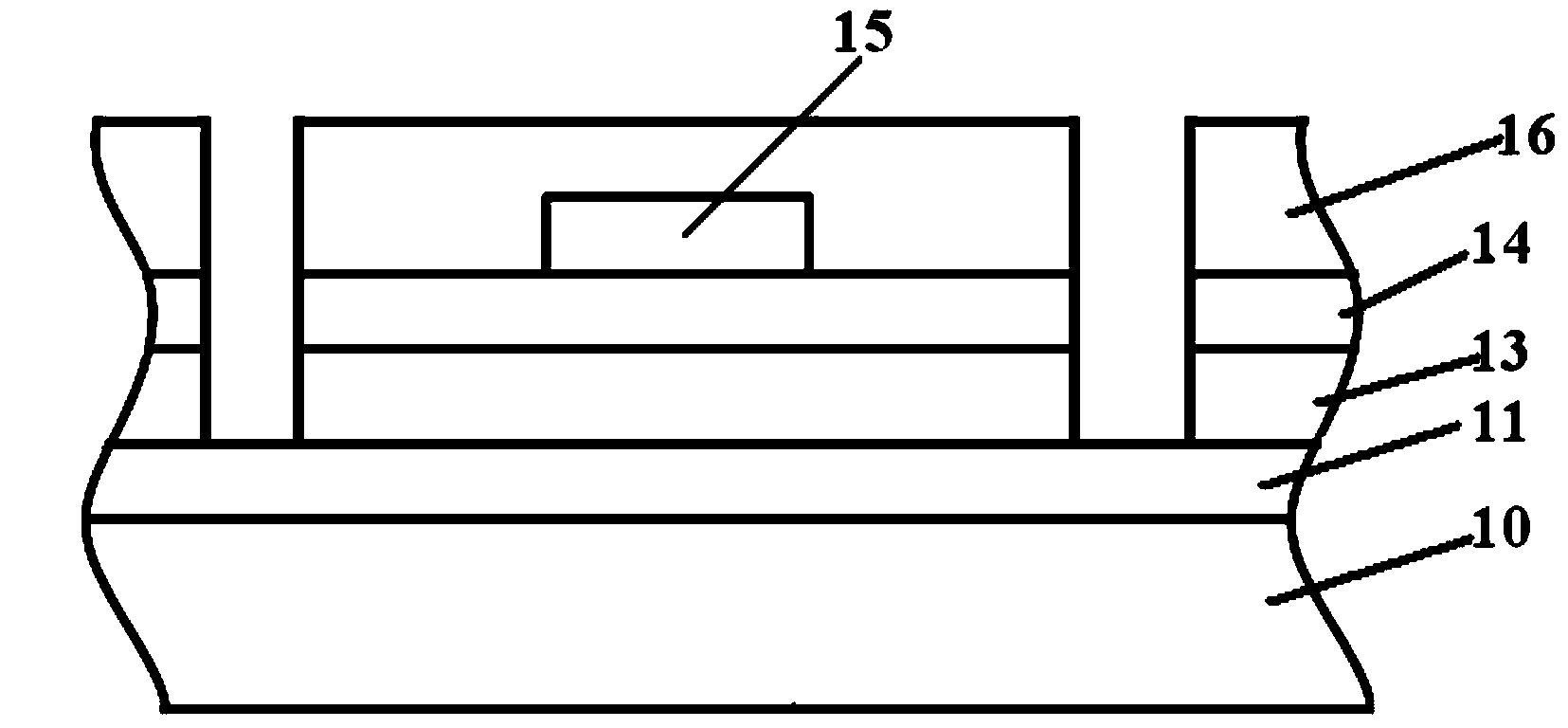
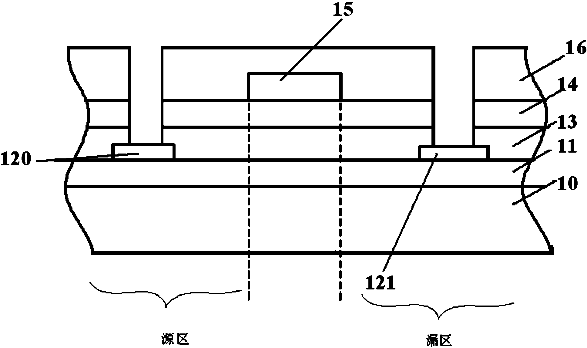
[0114] A low-temperature polysilicon thin film transistor array substrate with a top-gate structure can be manufactured through this embodiment, and the method for manufacturing the array substrate of this embodiment includes the following steps:

[0115] Step a1: providing a base substrate 10, and forming a buffer layer 11 on the base substrate 10;

[0116] Wherein, the base substrate 10 may be a glass substrate or a quartz substrate. Specifically, a plasma-enhanced chemical vapor deposition (PECVD) method can be used to deposit a thickness of about The buffer layer 11, wherein the material of the buffer layer can be selected from oxide, nitride or oxynitride, and the buffer layer can be a single-layer, double-layer or multi-layer structure. Specifically, the buffer layer may be SiNx, SiOx or Si(ON)x.

[0117] Step a2: forming conductive patterns 120, 121 capable of connecting to the active layer on the buffer layer 11 at positions corresponding to the contact holes;

[0...

Embodiment 2

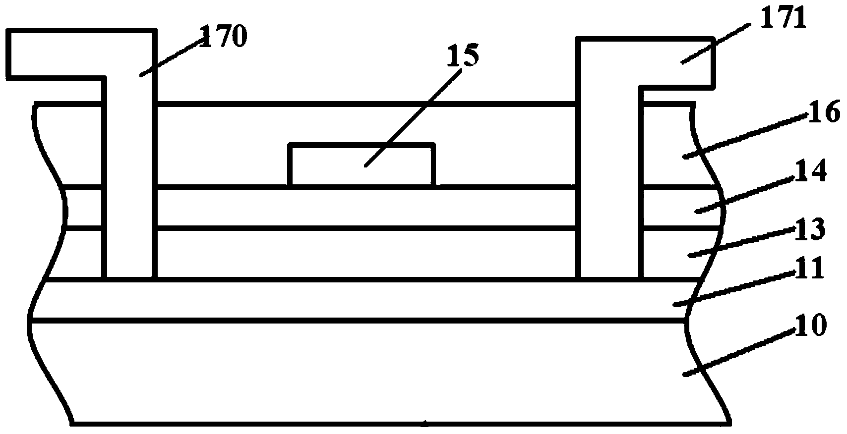
[0133] Through this embodiment, a low-temperature polysilicon thin film transistor array substrate with a bottom gate structure can be manufactured, and the method for manufacturing the array substrate of this embodiment includes the following steps:

[0134] Step b1: providing a base substrate, and forming a buffer layer on the base substrate;

[0135] Wherein, the base substrate may be a glass substrate or a quartz substrate. Specifically, the plasma-enhanced chemical vapor deposition (PECVD) method can be used to deposit a thickness of about The buffer layer, wherein the material of the buffer layer can be selected from oxide, nitride or oxynitride, and the buffer layer can be a single-layer, double-layer or multi-layer structure. Specifically, the buffer layer may be SiNx, SiOx or Si(ON)x.

[0136] Step b2: forming patterns of gate electrodes and gate lines on the base substrate after step b1 through a patterning process;

[0137] Specifically, a layer with a thickness...


PUM


Abstract

The invention provides a low-temperature polycrystalline silicon thin film transistor array substrate, a manufacturing method of the low-temperature polycrystalline silicon thin film transistor array substrate and a display device, and belongs to the field of the thin film transistor manufacturing technology. The low-temperature polycrystalline silicon thin film transistor array substrate comprises contact holes, wherein a source electrode and a drain electrode of the low-temperature polycrystalline silicon thin film transistor array substrate are connected with an active layer through the contact holes, and conductive patterns which are connected with the active layer are arranged at the bottoms of the contact holes. According to the technical scheme, good Ohmic contact can be formed between the source electrode of the low-temperature polycrystalline silicon thin film transistor array substrate and the active layer, and between the drain electrode of the low-temperature polycrystalline silicon thin film transistor array substrate and the active layer after etching of the contact holes is accomplished, and display quality of the display device is ensured.

Description

technical field [0001] The invention relates to the field of thin film transistor manufacturing technology, in particular to a low-temperature polysilicon thin film transistor array substrate, a manufacturing method thereof, and a display device. Background technique [0002] LTPS (low temperature polysilicon) has high carrier mobility due to its regular arrangement of atoms (10-300cm 2 / Vs), but also has a higher driving current, which can speed up the response time of liquid crystal, reduce the volume of TFT (thin film transistor), increase the transmission area, and obtain higher brightness and resolution. Therefore, the manufacturing process of thin film transistors is widely used. The active layer is prepared by LTPS. [0003] figure 1 with figure 2 Shown is a schematic structural diagram of an existing low-temperature polysilicon thin film transistor array substrate, wherein 10 is a substrate substrate, 11 is a buffer layer, 13 is an active layer, 14 is a gate insu...

Claims


Application Information

Patent Timeline
Patent Type & Authority Applications(China)
IPC IPC(8): H01L27/12H01L29/786H01L21/77
CPCH01L29/41733H01L29/458H01L29/78603H01L29/78675H01L27/1222H01L27/124H01L27/1262H01L29/78678
Inventor 左岳平刘政
Owner BOE TECH GRP CO LTD
Why Eureka
Try Eureka