Semiconductor device and manufacturing method thereof

A manufacturing method and semiconductor technology, applied in semiconductor devices, semiconductor/solid-state device manufacturing, electrical components, etc., can solve problems affecting the performance of semiconductor devices, equivalent oxide thickness, etc., to achieve superior performance and avoid impact effects

Inactive Publication Date: 2014-01-29
SEMICON MFG INT (SHANGHAI) CORP
View PDF7 Cites 3 Cited by
  • Summary
  • Abstract
  • Description
  • Claims
  • Application Information

AI Technical Summary

Problems solved by technology

[0013] However, the equivalent oxide thickness of the high-k gate dielectric layer of the semiconductor device fabricated by the above method is very thick, which ultimately affects the performance of the semiconductor device

Method used


Image

  • Semiconductor device and manufacturing method thereof
  • Semiconductor device and manufacturing method thereof
  • Semiconductor device and manufacturing method thereof

Examples


Embodiment Construction

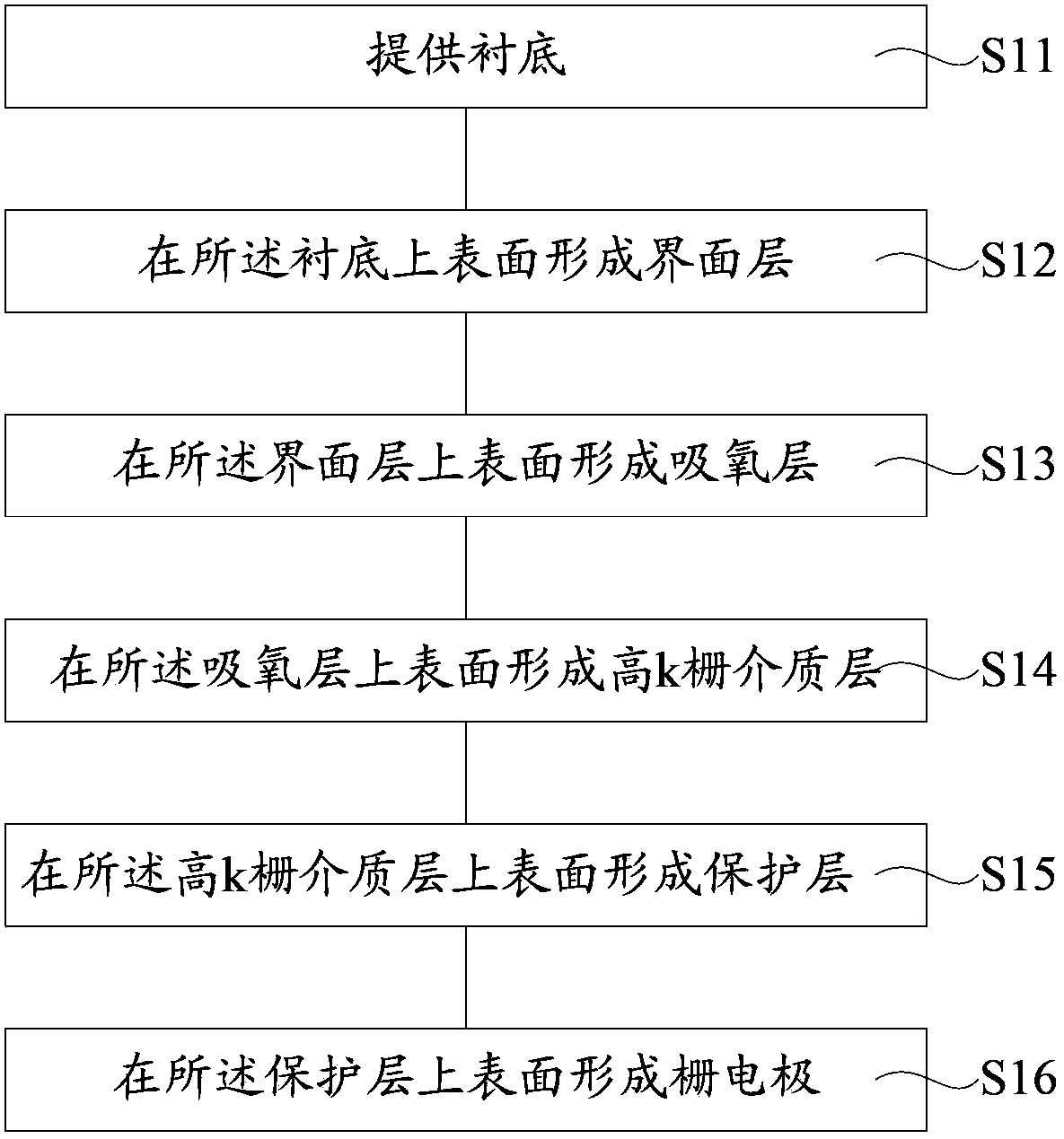
[0030] In order to make the above objects, features and advantages of the present invention more comprehensible, specific implementations of the present invention will be described in detail below in conjunction with the accompanying drawings.

[0031] In the following description, many specific details are set forth in order to fully understand the present invention, but the present invention can also be implemented in other ways than those described here, so the present invention is not limited by the specific embodiments disclosed below.

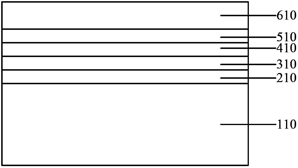
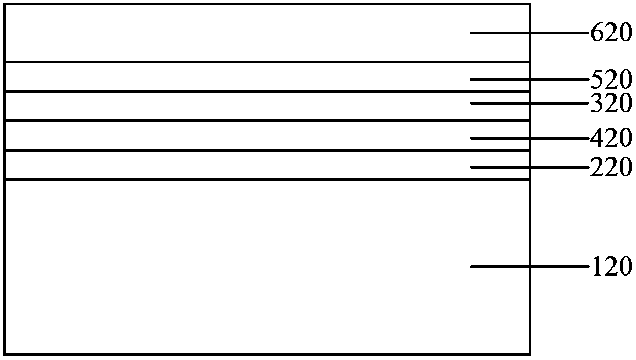
[0032] As mentioned in the background technology section, the equivalent oxide thickness of the high-k gate dielectric layer of the semiconductor device manufactured in the prior art is very thick, which ultimately affects the performance of the semiconductor device.

[0033] After research by the inventors, it was found that: since the substrate mostly includes shallow trench isolation structures (STI), and the shallow trench isolation st...


PUM


Abstract

Disclosed are a semiconductor device and a manufacturing method thereof. The semiconductor device comprises a substrate, a high k gate dielectric layer, an oxygen absorption layer and gate electrodes, wherein the high k gate dielectric layer is positioned on the upper surface of the substrate, the oxygen absorption layer is positioned on the upper surface or the lower surface of the high k gate dielectric layer, and the gate electrodes are positioned on the upper surface of the high k gate dielectric layer. The manufacturing method of the semiconductor device includes the steps: providing the substrate; forming the high k gate dielectric layer on the upper surface of the substrate; forming the oxygen absorption layer on the upper surface of the substrate or on the upper surface of the high k gate dielectric layer before or after forming the high k gate dielectric layer; forming the gate electrodes on the upper surface of the high k gate dielectric layer. The semiconductor device is provided with thin equivalent oxide, and the performance of the semiconductor device can be improved.

Description

technical field [0001] The invention relates to the technical field of semiconductors, in particular to a semiconductor device and a manufacturing method thereof. Background technique [0002] Nowadays, in lower process nodes, a gate stack structure combining a gate dielectric layer of a high-k material with a low equivalent oxide thickness (EOT, Equivalent Oxide Thickness) and a metal gate electrode is widely used. [0003] Regarding the formation method of the transistor with the high-K / metal gate structure, reference may be made to the US patent document with publication number US 2009 / 0142899 A1. [0004] In order to improve the interface characteristics between the high-k gate dielectric layer and the substrate, an interface layer (interfacial layer, IL) can be set between the substrate and the high-k gate dielectric layer. A better quality interface can also provide a better quality interface between the high-k gate dielectric layer and the interface layer. In additi...

Claims


Application Information

Patent Timeline
Patent Type & Authority Applications(China)
IPC IPC(8): H01L29/423H01L21/28
CPCH01L29/42364H01L21/283
Inventor 李凤莲倪景华
Owner SEMICON MFG INT (SHANGHAI) CORP
Why Eureka
Try Eureka