Wafer Back Process Method for Super Junction Devices

A backside process, super junction technology, used in semiconductor devices, semiconductor/solid-state device manufacturing, electrical components, etc., can solve problems such as residual defects and particles that cannot be cleaned, and achieve the effect of avoiding poor thickness uniformity

Active Publication Date: 2022-06-17
SHANGHAI HUAHONG GRACE SEMICON MFG CORP
View PDF3 Cites 0 Cited by
  • Summary
  • Abstract
  • Description
  • Claims
  • Application Information

AI Technical Summary

Problems solved by technology

[0004] Although the new back-sealing film structure will solve the problem of Auto Doping (self-doping, the doping elements on the back expand into the working process chamber during the process and then doped into the surface of the wafer, which affects the doping on the surface of the wafer. impurity concentration), but in the subsequent process, there will be granular residual defects on the back, which cannot be cleaned by normal cleaning machines

Method used


Image

  • Wafer Back Process Method for Super Junction Devices
  • Wafer Back Process Method for Super Junction Devices

Examples


Embodiment Construction

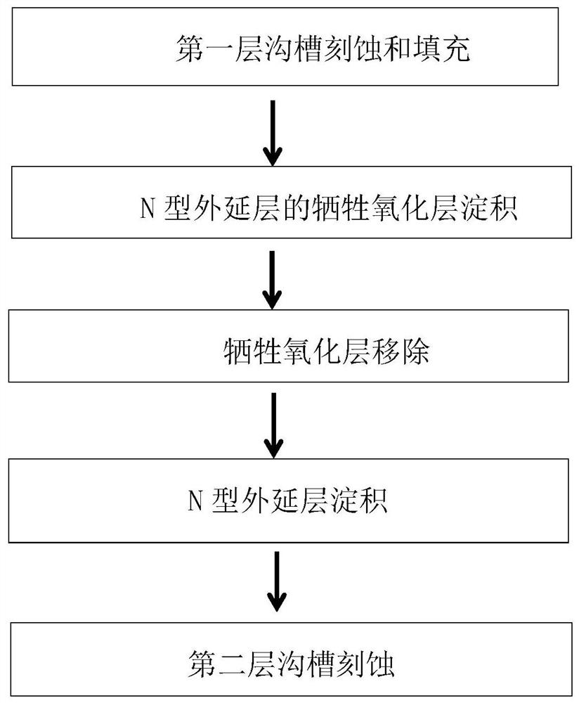
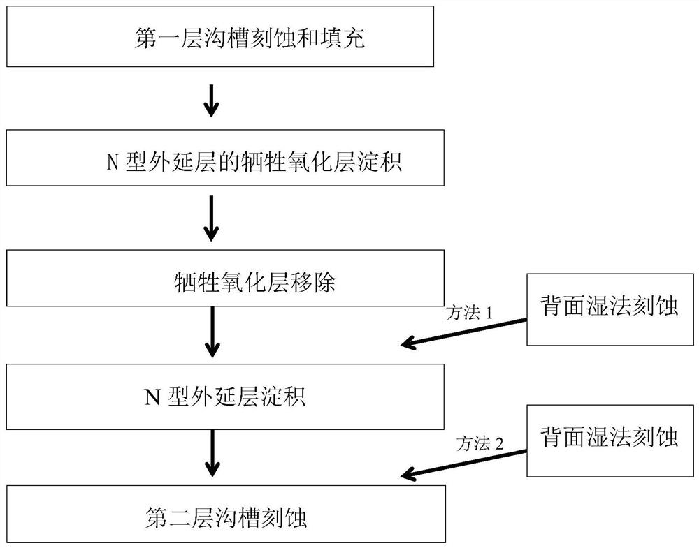
[0029] The process method for the backside of the wafer of the super junction device according to the present invention is a process of making the superjunction device on the wafer, and the backside of the wafer has been attached with a backside sealing film. It includes the following process steps:

[0030] In the first step, a first-layer trench is formed by etching on a semiconductor substrate, such as a silicon substrate or a silicon epitaxial layer, and is filled by epitaxial deposition.

[0031] In the second step, the sacrificial oxide layer is deposited on the N-type epitaxial layer. Since there may be some defects on the surface of the material, these defects can be eliminated by forming a sacrificial oxide layer.

[0032] In step 3, the sacrificial oxide layer is removed.

[0033] In the fourth step, a wet etching process of polysilicon on the backside of the wafer is performed. All polysilicon is etched away by wet etching on the backside. Make sure that there i...


PUM


Abstract

The invention discloses a wafer back process method for a super junction device, which is a process for manufacturing a super junction device on a wafer, comprising: a first step, etching and filling a first layer of trenches on a semiconductor substrate ; The second step is to deposit the sacrificial oxide layer of the N-type epitaxial layer; the third step is to remove the sacrificial oxide layer; the fourth step is to carry out the wet etching process on the back of the wafer; the fifth step is to carry out the N-type epitaxy Layer deposition; step 6, etching again to form a second layer trench. Alternatively, the wet etching process on the back of the wafer is performed after the deposition of N rows of epitaxial layers in the fifth step. The present invention adds back polysilicon wet etching before or after the growth of the N-type epitaxial layer, and can effectively avoid the influence on the thickness of the back sealing film layer during the operation of the N-type epitaxial layer before the growth of the N-type epitaxial layer , performing wet etching after the growth of the N-type epitaxial layer can effectively avoid the problem of poor thickness uniformity of the back sealing film layer.

Description

technical field [0001] The invention relates to the field of semiconductor manufacturing, in particular to a wafer backside processing method of a super junction device. Background technique [0002] The super junction product is a MOSFET structure that utilizes PN charge balancing in-vivo Resurf technology to increase the reverse breakdown voltage BV of the device while maintaining a small on-resistance. [0003] The super junction device replaces the N drift region in the traditional VDMOS by using the N / P alternate arrangement structure. It can be combined with the well-known VDMOS process in the industry to produce a super junction structure MOSFET. In the case of the same VDMOS, the on-resistance of the device is greatly reduced by using an epitaxial layer with low resistivity. The carrier distribution of the P-type impurities in the thin layer and the carrier distribution of the N-type impurities and their matching affect the characteristics of the device including it...

Claims


Application Information

Patent Timeline
Patent Type & Authority Patents(China)
IPC IPC(8): H01L21/336
CPCH01L29/66712
Inventor 杨继业赵龙杰李昊
Owner SHANGHAI HUAHONG GRACE SEMICON MFG CORP
Why Eureka
Try Eureka