Terahertz waveband broadband absorbing metamaterial
A terahertz and metamaterial technology, which is applied in the field of broadband absorption metamaterials in the terahertz band, can solve the problems of difficult processing and limited absorption bandwidth, and achieve the effect of low manufacturing precision requirements, easy mass production, and improved duty cycle.
- Summary
- Abstract
- Description
- Claims
- Application Information
AI Technical Summary
Problems solved by technology
Method used
Image
Examples
Embodiment 1
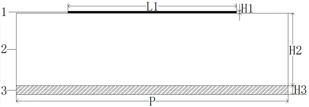
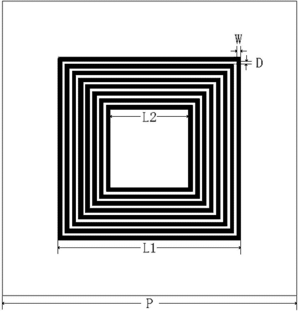
[0029] The terahertz band broadband absorbing metamaterial includes a metal reflective layer, a dielectric layer and a metal pattern layer. The metal reflection layer is a continuous metal aluminum film, the thickness of the reflection layer is H3=1μm, and the conductivity of metal aluminum is σ=3.56×10 7 S / m; the dielectric layer is polyimide, the thickness H2=9μm, the dielectric constant ε=3.5, the magnetic permeability is μ=1; the metal pattern layer is 8 concentric square metal rings, the concentric metal rings Metal section width W=0.4μm, height H1=0.05μm, distance between each metal ring is D=0.3μm, outermost square metal ring side length L1=19.6μm, innermost square ring side length L2=8μm, two-dimensional Periodic array metamaterial period is P=30μm. The preferred scheme of the metal pattern layer is as figure 2 shown.
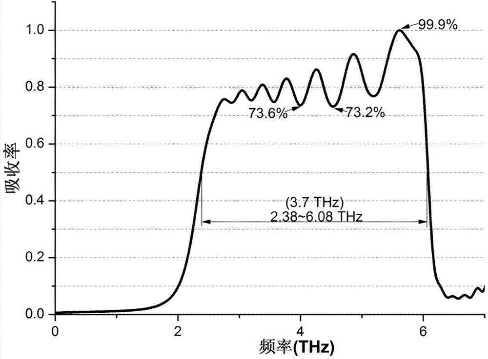
[0030] The above terahertz band broadband absorbing metamaterial has been simulated by CST, and its absorption spectrum is as follows: image 3 sh...
Embodiment 2
[0032] The terahertz band broadband absorbing metamaterial includes a metal reflective layer, a dielectric layer and a metal pattern layer. The metal reflection layer is a continuous metal aluminum film, the thickness of the reflection layer is H3=1μm, and the conductivity of metal aluminum is σ=3.56×10 7 S / m; the dielectric layer is polyimide, the thickness of the dielectric layer is H2=6μm, the dielectric constant ε=3.5, and the magnetic permeability is μ=1; the metal pattern layer is 8 concentric square metal rings, and the concentric metal The metal section width of the ring is W=0.2 μm, the height H1=0.04 μm, the distance between each metal ring is D=0.1 μm, the side length of the outermost square metal ring is L1=19.6 μm, and the side length of the innermost square ring is L2=14 μm. The period of the two-dimensional periodic array metamaterial is P=30μm. The preferred scheme of the metal pattern layer is as figure 2 shown.
[0033] The above terahertz band broadband ...
Embodiment 3
[0035]The broadband absorbing terahertz band broadband absorbing metamaterial includes a metal reflective layer, a dielectric layer and a metal pattern layer. The metal reflection layer is a continuous metal aluminum film, the thickness of the reflection layer is H3=1μm, and the conductivity of metal aluminum is σ=3.56×10 7 S / m; the dielectric layer is polyimide, the thickness of the dielectric layer is H2=10μm, the real permittivity ε=3.5, and the magnetic permeability is μ=1; the metal pattern layer is 8 concentric square metal rings, and the concentric The metal section width of the metal ring is W=0.6μm, the height H1=0.6μm, the distance between each metal ring is D=0.4μm, the side length of the outermost square metal ring is L1=19.6μm, and the side length of the innermost square ring is L2=3.3 μm, the period of the two-dimensional periodic array metamaterial is P=30μm. The preferred scheme of the metal pattern layer is as figure 2 shown.
[0036] The above terahertz b...
PUM
| Property | Measurement | Unit |
|---|---|---|
| height | aaaaa | aaaaa |
| thickness | aaaaa | aaaaa |
| thickness | aaaaa | aaaaa |
Abstract
Description
Claims
Application Information


