LED (light emitting diode) light source for plant growth

A technology for LED light source and plant growth, applied in the field of plant supplementary light source, can solve the problems of high cost and uneven light mixing of LED light source, and achieve a well-developed root system, good uniformity and consistency of light color, and enhanced resistance and immunity. Effect

Active Publication Date: 2014-02-12
WUXI HUAZHAOHONG OPTOELECTRONICS TECH
View PDF16 Cites 13 Cited by
  • Summary
  • Abstract
  • Description
  • Claims
  • Application Information

AI Technical Summary

Problems solved by technology

[0011] The purpose of the present invention is to solve the problems of uneven light mixing and high cost of LED light sources for plants in the prior art, and provide an LED light source that is used in conjunction with light-emitting chips and fluorescent powder to solve the above problems

Method used


Image

  • LED (light emitting diode) light source for plant growth
  • LED (light emitting diode) light source for plant growth
  • LED (light emitting diode) light source for plant growth

Examples


Embodiment 1

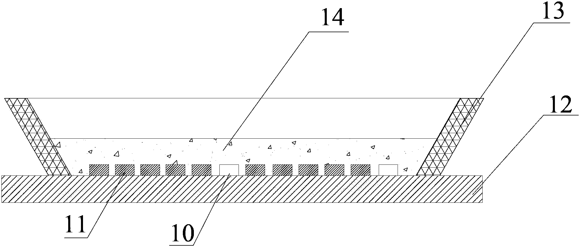
[0032] see figure 2 , on the ceramic heat dissipation substrate 22, use a dam dispenser to dispense glue to form a closed resin ring 23. The closed resin ring 23 can be square or circular. Other situations, such as rhombus or hexagon, are also allowed. In ceramic Several gallium nitride-based blue light chips 21 are mounted in the space formed by the heat dissipation substrate 22 and the closed dam 23. The gallium nitride-based blue light chips 21 are arranged in an array, and each row of gallium nitride-based blue light chips There are 12 chips 21 (but not limited to 12). Gallium nitride-based blue-ray chips 21 are sealed with silica gel, and then baked at 150°C for 1-3 hours to form a silica gel layer 24, and finally coat the surface of the silica gel layer 24 with Spread a layer of red phosphor powder 25, test its color coordinates when coating red phosphor powder 35, ensure that the color coordinates are near x==0.41, y==0.16, control the amount of red phosphor powder 35 ...

Embodiment 2

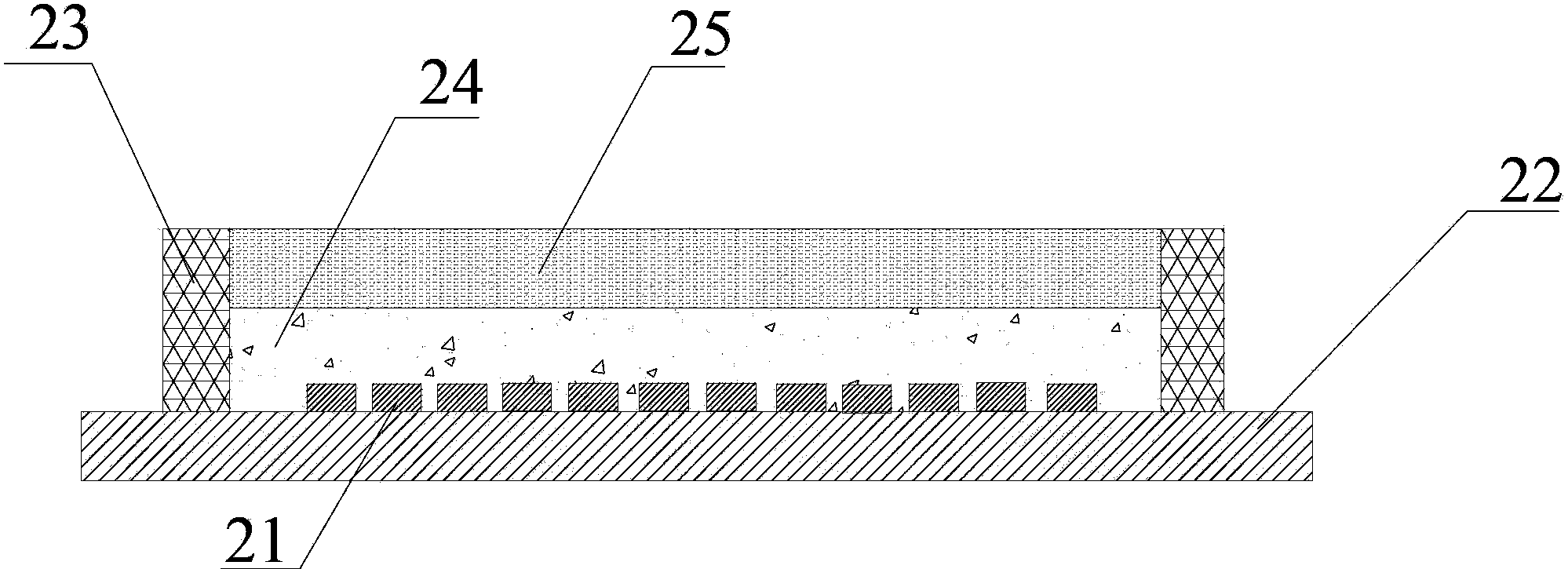
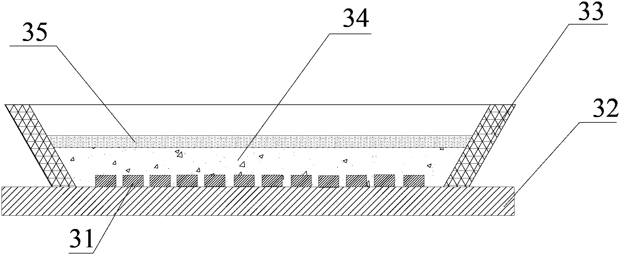
[0034] see image 3, above the metal-based heat dissipation substrate 32, a closed ring layer 33 formed of epoxy resin is fixed, and the closed resin ring layer 33 can be square or circular. Other situations, such as rhombus or hexagon, are also allowed. Several gallium nitride-based blue-ray chips 31 are mounted in the space formed by the heat-dissipating substrate 32 and the closed epoxy resin ring layer 33. The blue-ray chips 31 are arranged in an array, and each row of gallium nitride-based blue-ray chips 21 is 12 pieces (but not limited to 12 pieces), the gallium nitride-based blue-ray chip 31 is sealed with silica gel, and then baked at 150°C for 1-3 hours to form a silica gel layer 34, and finally coat a layer on top of the silica gel layer. Layer silicate-based red phosphor 35, test its color coordinates when coating red phosphor 35, ensure that the color coordinates are near x=0.41, y=0.16, control the amount of red phosphor 35 added through the color coordinates, aft...


PUM


Abstract

The invention discloses an LED (light emitting diode) light source for plant growth. The LED light source for plant growth comprises a radiating substrate and a sealing ring, wherein the sealing ring is arranged on the surface of the radiating substrate; a plurality of gallium-nitride-based blue light chips are arranged on the surface of the radiating substrate and are positioned in a closed area surrounded by the sealing ring; a silica gel layer is hermetically arranged on each gallium-nitride-based blue light chip; and red phosphor is coated on the surfaces of the silica gel layers. The LED light source for plant growth has the advantages that according to a plant growth and development rhythm, a photosynthesis principle and difference of plants on light spectrum sensitivity, light can be scientifically and reasonably supplemented for plants during growth by using a principle that the plants selectively absorb spectral wavelength during growth, sufficient photosynthesis of the plants is ensured, laminas of the plants are thick, roots of the plants are well developed, and the plants grow well; the strength and the immunity of the plants are enhanced; precocity and yield increasing of the plants are promoted; and the quality of the plants is improved.

Description

technical field [0001] The present invention relates to the field of semiconductor lighting technology and the field of plant growth technology. Specifically, it is a plant that uses a solid light-emitting chip of a specific wave band to excite phosphor powder of a specific wave band, and combines the two into a solid light source to promote plant growth and improve plant quality. Fill light source. Background technique [0002] With the gradual improvement of people's living standards and changes in food demand, more and more attention has been paid to healthy, green, environmentally friendly and convenient lifestyles. Hygienic, nutritious and healthy food has become more and more popular among people, among which green and pollution-free , Fresh and clean vegetable products are particularly important to people's modern life. And how to produce this vegetable quickly and with good quality and quantity has become an important issue that people pay close attention to. [00...

Claims


Application Information

Patent Timeline
Patent Type & Authority Applications(China)
IPC IPC(8): F21S19/00A01G9/20F21Y101/02F21Y113/17F21Y115/10
Inventor 李杰民常保延李震球李鹏
Owner WUXI HUAZHAOHONG OPTOELECTRONICS TECH
Why Eureka
Try Eureka