An Electron Beam Exposure Method for Improving the Uniformity of Grating Structure

A technology of grating structure and uniformity, which is applied in microlithography exposure equipment, diffraction gratings, photolithographic process exposure devices, etc., can solve problems such as electron scattering and superposition, and achieve the effect of improving exposure uniformity.

Inactive Publication Date: 2015-11-18
INST OF SEMICONDUCTORS - CHINESE ACAD OF SCI
View PDF4 Cites 0 Cited by
  • Summary
  • Abstract
  • Description
  • Claims
  • Application Information

AI Technical Summary

Problems solved by technology

Especially in densely arranged or arrayed nanometer-scale graphics, it will cause the superposition of electron scattering, resulting in graphic deformation or graphic connection.

Method used


Image

  • An Electron Beam Exposure Method for Improving the Uniformity of Grating Structure
  • An Electron Beam Exposure Method for Improving the Uniformity of Grating Structure
  • An Electron Beam Exposure Method for Improving the Uniformity of Grating Structure

Examples


Embodiment Construction

[0020] In order to make the object, technical solution and advantages of the present invention clearer, the present invention will be further described in detail below in conjunction with specific embodiments and with reference to the accompanying drawings.

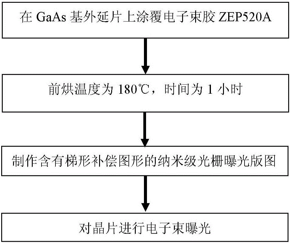
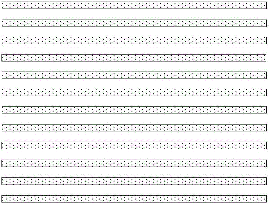
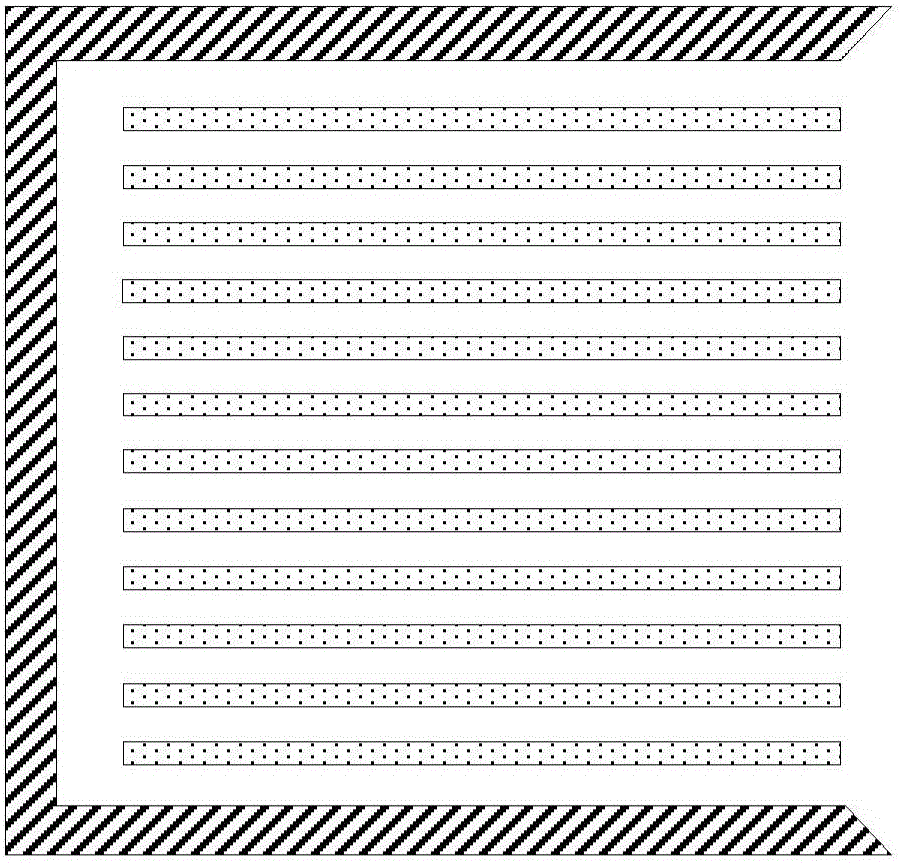
[0021] The method for improving the exposure uniformity of the grating provided by the present invention arranges trapezoidal compensation patterns around the original nanoscale grating, which reduces the influence of the proximity effect on the pattern, so that each grating bar is not deformed and superimposed. The nanoscale gratings are densely arranged in submicron order period, and the edges of the pattern are smooth.

[0022] figure 1 A flow chart of an electron beam exposure method for improving grating exposure uniformity according to an embodiment of the present invention is shown. Such as figure 1 As shown, this embodiment takes a GaAs-based epitaxial wafer as an example, and the method includes the following s...


PUM

PropertyMeasurementUnit
widthaaaaaaaaaa

Abstract

The invention discloses a method for improving the uniformity of a grating, and particularly relates to an electron beam exposure method for improving the uniformity of a grating structure. The method comprises the steps that electron beam glue coats a wafer, and the wafer coated with the electron beam glue is placed in a baking oven to be prebaked; trapezoid compensatory figures are arranged around the grating structure by utilizing a layout design tool; electron beam exposure and development are carried out on the wafer to finish the grating structure containing the trapezoid compensatory figures. By utilizing the compensatory figures, the method weakens the influence of the proximity effect in the electron beam exposure, and the uniformity of nanometer-scale grating exposure is increased. Instead of weakening the proximity effect by changing the exposure dose and size of a figure, the proximity effect is weakened by increasing the compensatory figures around the figure in order to improve the grating exposure uniformity.

Description

technical field [0001] The invention relates to the processing field of nanoscale microfabrication technology, in particular to an electron beam exposure pattern compensation method for improving the uniformity of nanoscale gratings. Background technique [0002] Electron beam lithography is widely used in nanoelectronics and optoelectronic devices. Electron beam exposure uses a high-energy focused electron beam to directly draw or project a reproduced pattern on a resist-coated substrate. Since the de Broglie wavelength range of the electrons in the electron beam is 0.04-0.1 Angstroms, the resolution is not affected by diffraction effects. Electron beam exposure can ensure accurate graphics and smooth edges in the range of 50-500nm. In fact, the resolution of electron beam exposure mainly depends on the electron beam spot size determined by the electron optical system, the proximity effect, the characteristics of the electron beam glue and the development method and other...

Claims


Application Information

Patent Timeline
Patent Type & Authority Patents(China)
IPC IPC(8): G02B5/18G03F7/00G03F7/20B82Y10/00B82Y40/00
Inventor 王莉娟喻颖査国伟徐建星倪海桥牛智川
Owner INST OF SEMICONDUCTORS - CHINESE ACAD OF SCI
Why Eureka
Try Eureka