Method for improving VCSEL exposure uniformity and VCSEL chip

A technology of uniformity and exposure area, which is applied in a method of improving the uniformity of VCSEL exposure and in the field of VCSEL chips, which can solve the problems of affecting the exposure focus of the lithography process, affecting the resolution of graphics, and the inability of light to focus, so as to improve the quality of graphics , Improving exposure uniformity and improving yield

Pending Publication Date: 2021-11-30
华芯半导体研究院(北京)有限公司 +1
View PDF4 Cites 0 Cited by
  • Summary
  • Abstract
  • Description
  • Claims
  • Application Information

AI Technical Summary

Problems solved by technology

[0003] At present, the general VCSEL manufacturing process involves multiple processes such as photolithography, coating, etching, and oxidation. These processes generally undergo heating and cooling processes when etching or depositing metal and nitride films. After multiple related processes, a certain stress will cause the wafer to warp. When the warpage is serious, it will directly affect the exposure focus of the photolithography process. At this time, the light cannot be focused to the midpoint of the photoresist film and deviates from the Very far, affecting the resolution of the pattern after photoresist development, thus forming defects on the wafer

Method used


Image

  • Method for improving VCSEL exposure uniformity and VCSEL chip
  • Method for improving VCSEL exposure uniformity and VCSEL chip
  • Method for improving VCSEL exposure uniformity and VCSEL chip

Examples


Embodiment 1

[0055] During the VCSEL manufacturing process, the wafer (with a thickness of 100mm) will show a certain amount of warpage after undergoing high-temperature processes such as metal process, oxidation process, etc. , the wafer warpage value test method is as follows:

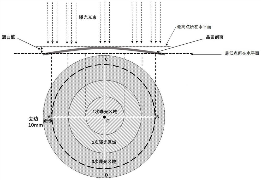
[0056] like figure 2 As shown, the horizontal axis AB and the vertical axis CD are vertically intersected through the point O of the wafer center. The horizontal axis intersects the outer edge of the wafer at points A and B, and the vertical axis intersects the outer edge of the wafer at points C and D. Since edge removal is performed during the actual chip process, points A, B, C, and D are each 10mm away from the edge.

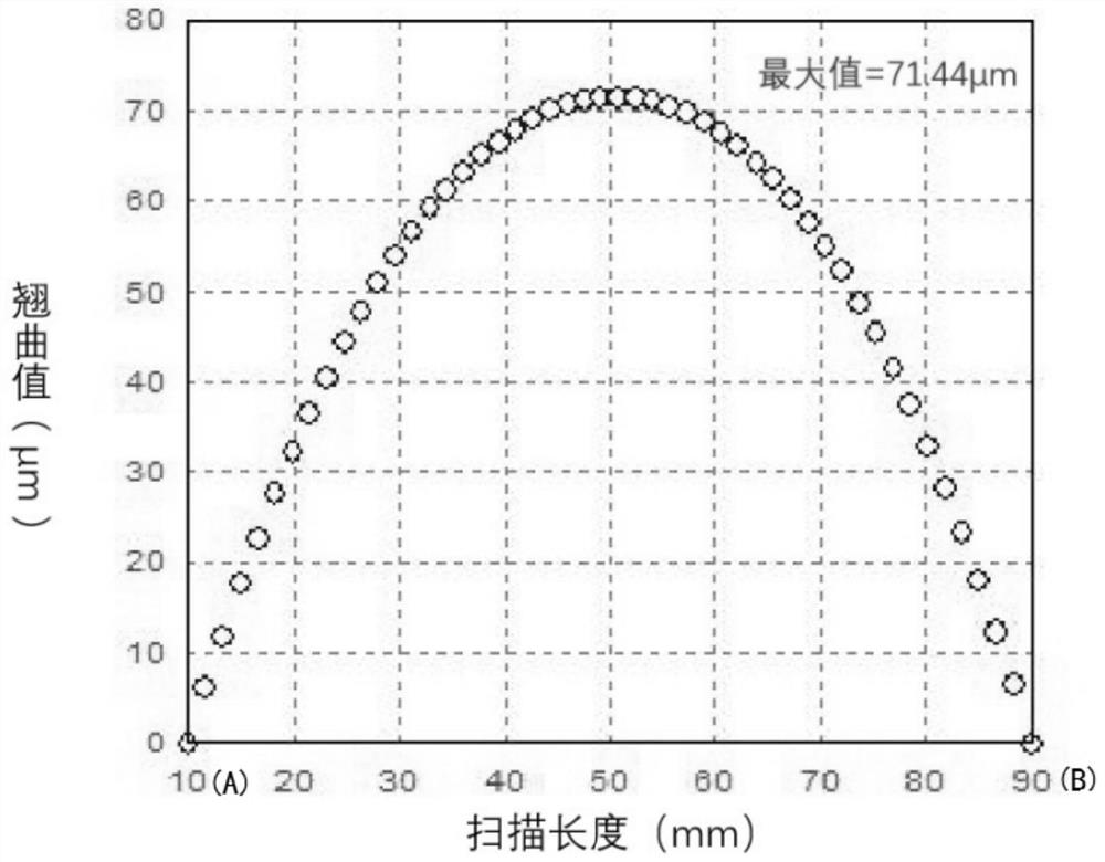
[0057] After the oxidation process is completed, use a film stress tester to scan the warpage value of the test wafer along the horizontal axis AB and the longitudinal axis CD respectively. The results of the AB line scan are shown in the attached image 3 As shown, the maximum warpage value...


PUM


Abstract

The invention discloses a method for improving VCSEL exposure uniformity and a VCSEL chip, and the method comprises the steps: (1) measuring a warping value of a to-be-photoetched surface of a wafer, wherein the warping value is a height difference between a horizontal plane where a highest point of the to-be-photoetched surface is located and a horizontal plane where a lowest point of the to-be-photoetched surface is located; (2) dividing the surface to be photoetched into at least two exposure areas according to the warping value; (3) respectively carrying out exposure in the at least two exposure areas. By adopting the exposure method disclosed by the invention, the exposure uniformity of the photoetching process can be effectively improved, the pattern quality is improved, the yield is improved, and the exposure method is simple to operate and easy to implement.

Description

technical field [0001] The invention relates to the technical field of VCSEL chip manufacturing, in particular, the invention relates to a method for improving VCSEL exposure uniformity and a VCSEL chip. Background technique [0002] Vertical cavity surface emitting laser (Vertical Cavity Surface Emitting Laser, VCSEL) is different from other light sources such as LED (Light Emitting Diode, light emitting diode) and LD (Laser Diode, laser diode), with small size, circular output spot, single longitudinal It has been widely used in the fields of optical communication, optical interconnection, and optical storage due to its advantages of low-mode output, low threshold current, and easy integration into large-area arrays. With the continuous development of science and technology, various VCSEL chips have been widely used in people's daily life, work and industry, bringing great convenience to people's life. [0003] At present, the general VCSEL manufacturing process involves ...

Claims


Application Information

Patent Timeline
IPC IPC(8): H01S5/183G03F7/20
CPCH01S5/183G03F7/2022
Inventor 钱旭王青江蔼庭吕朝晨赵风春王光辉
Owner 华芯半导体研究院(北京)有限公司
Why Eureka
Try Eureka