Method for automatically compensating pose errors in machining process of optical element

An optical element and automatic compensation technology, which is applied in the direction of instruments, computer control, simulators, etc., can solve the problems of large-caliber optical elements, laborious adjustment process, time-consuming adjustment process, cumbersome adjustment process, etc., to achieve fast compensation process, short time consumption, The effect of narrowing your search

Inactive Publication Date: 2014-02-19
CHANGCHUN INST OF OPTICS FINE MECHANICS & PHYSICS CHINESE ACAD OF SCI
View PDF5 Cites 18 Cited by
  • Summary
  • Abstract
  • Description
  • Claims
  • Application Information

AI Technical Summary

Problems solved by technology

The advantage of this traditional method is that it is easy to operate and the equipment is simple, but it has the following disadvantages and shortcomings: the adjustment accuracy is relatively low, and the edge runout can generally only be adjusted to about 5-10 μm; the adjustment process is highly skilled and difficult for the staff. The experience dependence is strong; the adjustment process is time-consuming and laborious, and the adjustment of large-aperture optical elements is laborious, and there is a risk of damage to the workpiece; when there is a large wedge angle between the upper and lower surfaces of the optical element or the adjusted surface is aspherical, the adjustment process will be very difficult cumbersome or even impossible

Method used


Image

  • Method for automatically compensating pose errors in machining process of optical element
  • Method for automatically compensating pose errors in machining process of optical element
  • Method for automatically compensating pose errors in machining process of optical element

Examples


Embodiment Construction

[0042] Below in conjunction with accompanying drawing and specific embodiment the present invention is described in further detail:

[0043] The method for automatically compensating pose error in optical element processing of the present invention comprises the following steps:

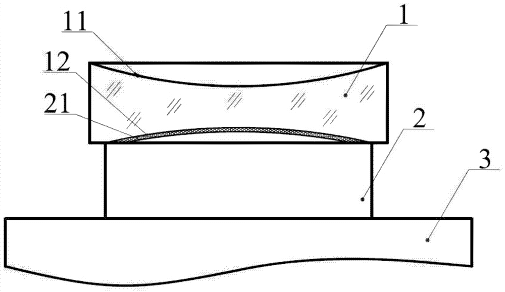
[0044] (1) Clamp the optical element 1 on the workbench 3:

[0045] Such as figure 1 As shown, the optical element 1 is clamped on the vacuum adsorption fixture 2, the upper surface 11 of the optical element is the surface to be processed, and the lower surface 12 is the mounting and positioning surface. The lower surface 12 is in close contact with the suction surface 21 of the vacuum suction fixture 2 . The vacuum adsorption fixture 2 is fixedly installed on the machine tool table 3, and the two are in a coaxial relationship. Since the lower surface 12 of the optical element 1 is a spherical surface, the optical element 1 will produce certain tilt errors and translation errors. When clamping th...


PUM


Abstract

The invention discloses a method for automatically compensating pose errors in the machining process of an optical element, relates to the machining field of optical elements, and aims to provide a method for automatically eliminating installation errors without adjusting a workpiece. The method adopts the following steps that the optical element is firstly clamped on a working table of a machine tool, and the surface of the optical element is measured; actual position measuring points are then transformed to be theoretical position measuring points according to a pose error vector construction transformation matrix; an objective function for solving pose error vectors and a solving mathematic model are built, and the pose errors are solved; a transformation matrix is built according to solutions of the pose errors, and position vectors and direction vectors of resident points on machining paths are transformed respectively; finally, the transformed resident points are subjected to post-processing to obtain a machining program after pose error compensating. The method can accurately and rapidly compensate the pose errors of the optical element and is suitable for being applied to the field of optical machining controlled by a computer.

Description

technical field [0001] The invention relates to the field of optical element processing, in particular to a method for automatically compensating installation pose errors in optical element processing. Background technique [0002] With the development of optical technology, higher and higher requirements are put forward for the processing quality of the surface of optical components. In the process of optical processing, the installation error of optical components is one of the important factors affecting the processing accuracy of optical components. Taking a processing machine tool with a rotary table as an example, the traditional method of eliminating installation errors is to use a mechanical watch to detect the runout of the edge of the workpiece, and then repeatedly adjust the position of the workpiece to reduce the installation error. The advantage of this traditional method is that it is easy to operate and the equipment is simple, but it has the following disadv...

Claims


Application Information

Patent Timeline
Patent Type & Authority Applications(China)
IPC IPC(8): G05B19/404
Inventor 刘健王绍治张玲花隋永新杨怀江
Owner CHANGCHUN INST OF OPTICS FINE MECHANICS & PHYSICS CHINESE ACAD OF SCI
Why Eureka
Try Eureka