Multi-layer multi-chip fan-out structure and manufacturing method
A multi-chip and die technology, applied in semiconductor/solid-state device manufacturing, electrical components, electric solid-state devices, etc., can solve problems such as chip shift and low alignment accuracy, and achieve optimized package size, compact package size, and low price Obvious effect
- Summary
- Abstract
- Description
- Claims
- Application Information
AI Technical Summary
Problems solved by technology
Method used
Image

Examples
Embodiment Construction
[0042] The present invention will be further described below in conjunction with specific drawings and embodiments.
[0043] Such as Figure 11 Shown:
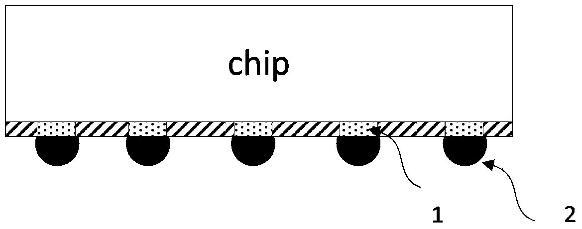
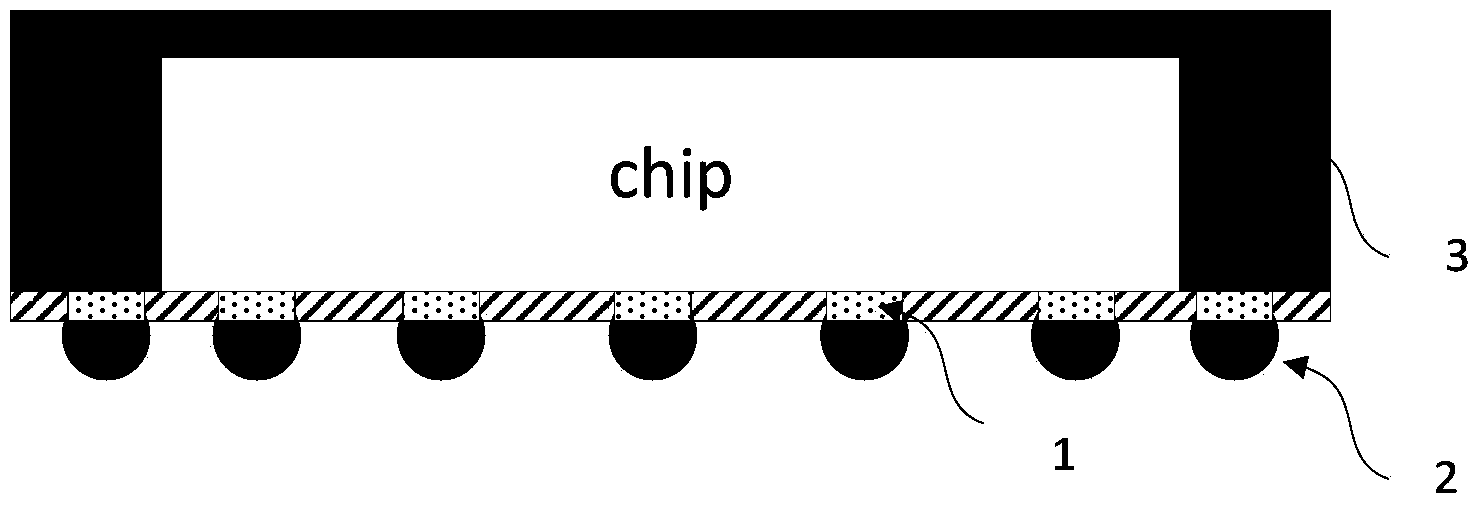
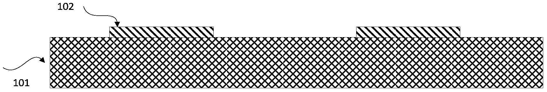
[0044] A multi-layer multi-chip fan-out structure, including a carrier board 101, on which a plurality of stacked package sub-bodies are arranged; each package sub-body is packaged with at least one die 201; in each package sub-body Among them, one or more dies 201 are covered by the dielectric material of the dielectric layer 103, and the dies 201 are mounted on the metal pad 102 in a face-up manner; There is an RDL layer 104; the solder pad on the front side of the die 201 is electrically connected to the RDL layer 104 of the package sub-body where the die 201 is located through the first interconnection hole 202'.
[0045] An insulating layer 105 is provided between adjacent package sub-bodies, and the RDL layers 104 of adjacent package sub-bodies are electrically connected through the second interconnection hole 203' bet...
PUM
 Abstract
Description
Claims
Application Information