Supercharge Your Innovation With Domain-Expert AI Agents!

Method of manufacturing multilayer ceramic electronic part

A technology of electronic components and manufacturing methods, which is applied in the manufacture of capacitors, components of fixed capacitors, electrical components, etc., can solve problems such as thinning and cannot be coated smoothly, and achieve the effect of stable electrical characteristics

Active Publication Date: 2014-02-19
MURATA MFG CO LTD
View PDF3 Cites 3 Cited by
  • Summary
  • Abstract
  • Description
  • Claims
  • Application Information

AI Technical Summary

Problems solved by technology

[0008] However, even if the paste for the insulator part is shared with the ceramic material used in the laminated body on the side surface of the laminated body chip, and a solvent that does not dissolve the laminated body is used, there is a problem that the above-mentioned In the case of applying the paste for the insulator portion to the side surface of the laminated chip by the conventional method as described above, the coating thickness on the edges of the laminated chip exceeds the allowable range for maintaining electrical characteristics and becomes thinner, or cannot be smoothed. Coating, etc.

Method used


Image

  • Method of manufacturing multilayer ceramic electronic part
  • Method of manufacturing multilayer ceramic electronic part
  • Method of manufacturing multilayer ceramic electronic part

Examples


Embodiment 1

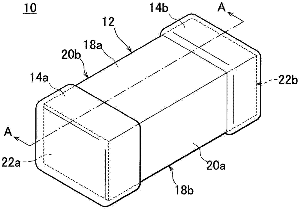
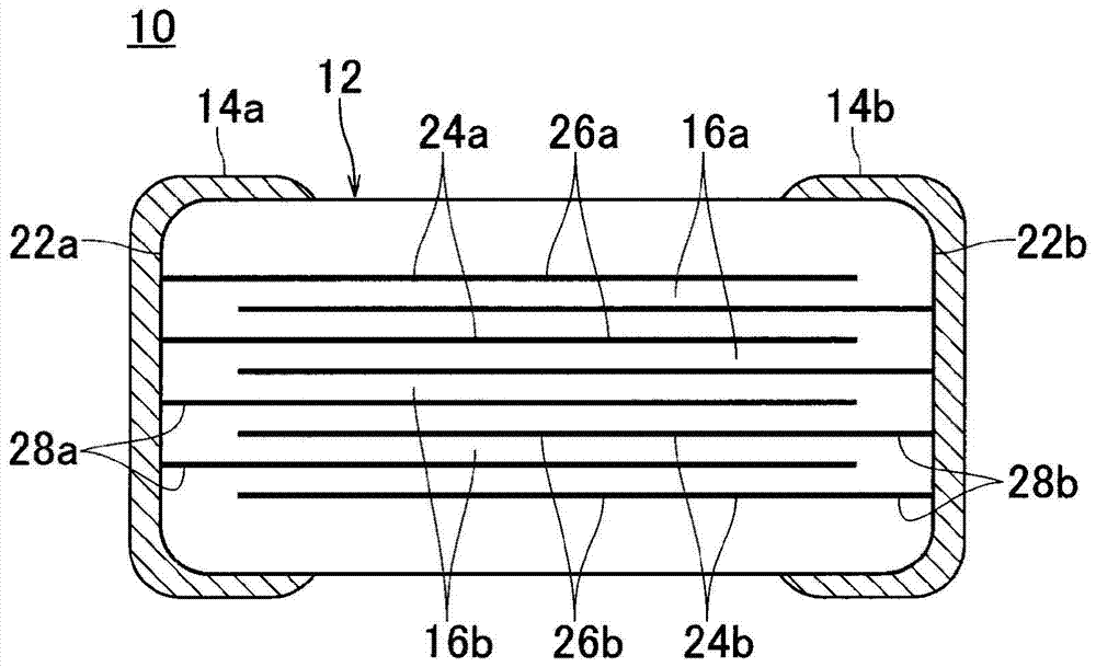
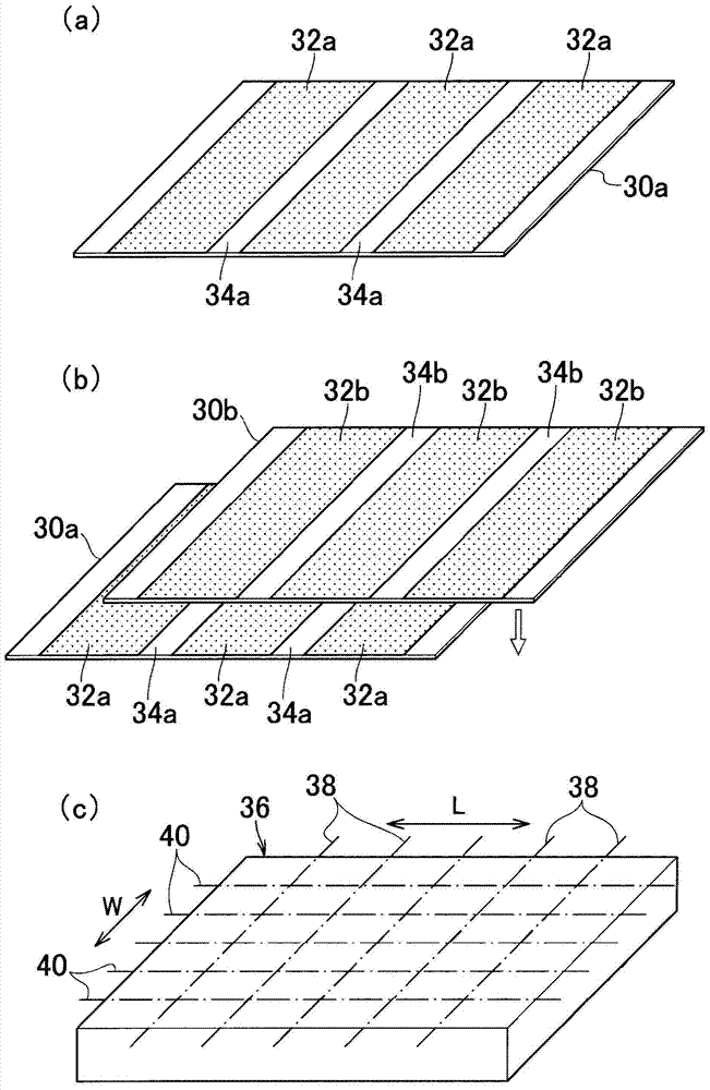
[0100] Next, an example related to a method of manufacturing a laminated ceramic electronic component according to the present invention will be described. The method of manufacturing a laminated ceramic electronic component according to this example is a method of printing stripe-shaped electrodes on a plurality of ceramic green sheets and laminating them, and cutting the laminated body to form a laminated body chip in which the electrodes on the side surfaces are exposed. , and then press this laminated body chip against a metal plate having a groove having an arbitrary volume filled with the paste for an insulator portion, thereby manufacturing a laminated ceramic electronic component.

[0101]In this example, the type of binder, the molecular weight of the binder, the content of the ceramic raw material, and the volume fraction of the ceramics were changed, and the paste for the insulator part in which the viscosity of the paste for the insulator part was changed was trial-...

Embodiment 2

[0153] Next, another embodiment related to the method of manufacturing a laminated ceramic electronic component according to the present invention will be described. The method of manufacturing a laminated ceramic electronic component according to this example is the same as in Example 1: a plurality of ceramic green sheets are printed with electrodes in stripes and laminated, and the laminated body is cut to expose the side surface. A multilayer chip of the electrode of the part is pressed against a metal plate having a groove such as a groove filled with an arbitrary volume of the paste for the insulator part, thereby manufacturing a laminated ceramic electronic component.

[0154] An example of the present invention is shown in a laminated ceramic electronic component in which polyvinyl butyral having a high molecular weight and a large number of hydroxyl groups is used as a binder for ceramic green sheet molding. Paste for insulator parts is prepared by using a solvent inc...


PUM

PropertyMeasurementUnit
viscosityaaaaaaaaaa
molecular weightaaaaaaaaaa

Abstract

[Problem] To provide a method of manufacturing a multilayer ceramic electronic part such that by providing a desired insulator section thickness for side faces of a multilayer chip, a multilayer ceramic electronic part having stable electrical characteristics and high-reliability can be obtained. [Solution] Provided is a method of manufacturing a multilayer ceramic electronic part, said method comprising: a process for preparing multilayer chips that are formed such that both side end-edges of internal electrodes are exposed at the side faces thereof; a process for forming a first insulator section and a second insulator section by pressing one side face and the other side face of the multilayer chips onto a metal plate, which comprises slots having an arbitrary volume and having an insulator-section paste filled into the slots having the arbitrary volume, and oscillating the metal plate in an arbitrary direction when separating the multilayer chips from the metal plate; and a process for firing the multilayer chips having the first insulation section and the second insulation section formed thereon. The insulator-section paste is characterized by having a viscosity of 500 Pa·s-2,500 Pa·s, and by the inorganic-solid-constituent content (C) (vol%) thereof satisfying a prescribed condition.

Description

technical field [0001] The present invention relates to a method of manufacturing laminated ceramic electronic components such as laminated ceramic capacitors. Background technique [0002] Conventionally, a multilayer chip before firing a multilayer ceramic electronic component was manufactured by printing a plurality of internal electrodes equivalent to one multilayer chip vertically and horizontally on a ceramic green sheet, and stacking and pressing the ceramic green sheets according to the required number. Afterwards, dicing is performed into individual chip shapes. In this method, in relation to the accuracy of the lamination position of the ceramic green sheet or the positional accuracy of the shape for dicing the laminate chip, it is necessary to ensure that the insulator portion on the side surface (the surface without the lead-out electrode) of the laminate chip has A certain width. Therefore, there are problems such as that the size of the multilayer chip may in...

Claims


Application Information

Patent Timeline
Patent Type & Authority Applications(China)
IPC IPC(8): H01G4/30H01G4/12H01G4/224
CPCH01G4/12H01G4/224H01G4/30B32B37/00B32B38/0004C04B37/00C04B2237/00C04B2237/12H01G7/00H01G13/00
Inventor 浜中建一伊藤英治山下泰治冈岛健一松井透悟
Owner MURATA MFG CO LTD
Features
  • R&D
  • Intellectual Property
  • Life Sciences
  • Materials
  • Tech Scout
  • Unparalleled Data Quality
  • Higher Quality Content
  • 60% Fewer Hallucinations
Learn More