Waveguide electro-optic modulator and manufacturing method thereof

An electro-optic modulator and manufacturing method technology, which are applied in the fields of instruments, optics, nonlinear optics, etc., can solve the problems of reducing modulation efficiency, difficult to further reduce the half-wave voltage, disadvantageous to low-power electro-optic modulation devices, etc., so as to reduce the impact, The effect of improving modulation characteristics

Active Publication Date: 2016-02-10
TSINGHUA UNIV
View PDF5 Cites 0 Cited by
  • Summary
  • Abstract
  • Description
  • Claims
  • Application Information

AI Technical Summary

Problems solved by technology

But this structure has a defect: the SI-InP layer is relatively thick, and a large part of the voltage needs to be divided, which reduces the modulation efficiency, making it difficult to further reduce the half-wave voltage, which is not conducive to the realization of low-power electro-optic modulation devices.

Method used


Image

  • Waveguide electro-optic modulator and manufacturing method thereof
  • Waveguide electro-optic modulator and manufacturing method thereof
  • Waveguide electro-optic modulator and manufacturing method thereof

Examples


Embodiment 1

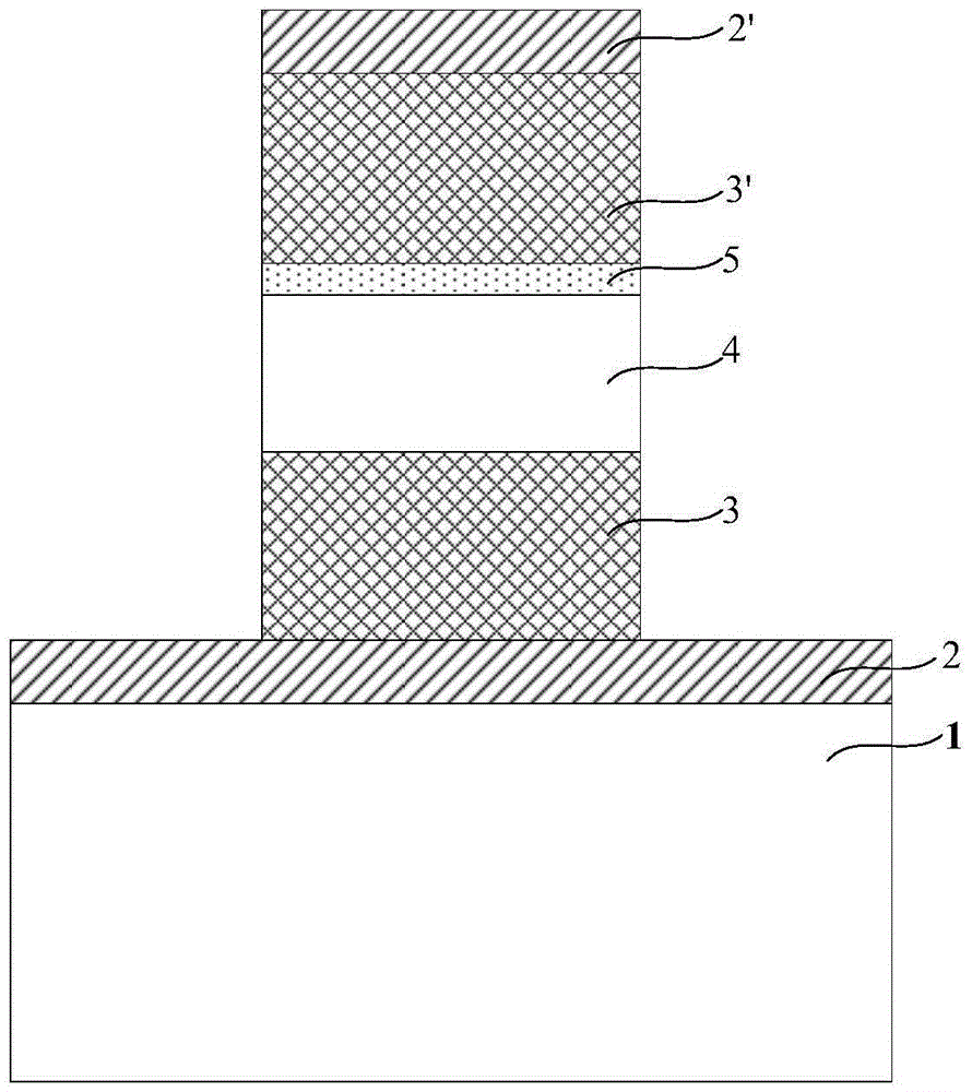
[0043] figure 2 It is a schematic structural diagram of a waveguide electro-optic modulator according to an embodiment of the present invention. Such as figure 2 As shown, it is InP-InGaAlAs / InAlAs-SiO 2 - Si (N-I-O-N type) ridge waveguide structure electro-optic modulator.

[0044] Specifically, there are two production methods.

[0045] The first production method includes the following steps:

[0046] Step 11, sequentially forming a device with an upper N-type semiconductor cladding layer, a semiconductor core layer and an insulator layer on the substrate;

[0047] Step 12. Surface-bond the insulator layer of the device on a (silicon-on-insulator) SOI substrate by surface bonding technology; wherein, the SOI substrate includes a silicon substrate, a silicon dioxide A silicon buried oxide layer and an N-type doped silicon layer, where the N-type doped silicon layer serves as a lower N-type semiconductor cladding layer;

[0048] Step 13, respectively forming an upper ...

Embodiment 2

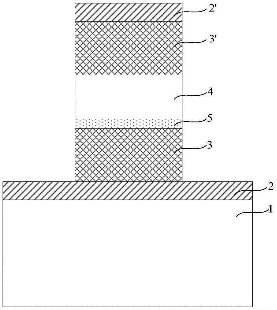
[0064] image 3It is a schematic structural diagram of a waveguide electro-optic modulator according to Embodiment 2 of the present invention. Such as image 3 As shown, it is InP-InGaAsP / InP-Al 2 o 3 - InP (N-I-O-N type) ridge waveguide structure electro-optic modulator.

[0065] The preparation method comprises the following steps:

[0066] Step 31, growing a lower N-type semiconductor cladding layer, a semiconductor core layer, a semiconductor layer containing Al, and an upper N-type semiconductor cladding layer sequentially on the substrate;

[0067] Step 32. Oxidize or nitride the Al-containing semiconductor layer into Al2O3 by lateral oxidation or nitridation 2 o 3 or aluminum nitride AlN insulator layer;

[0068] Step 33, respectively forming an upper electrode on the surface of the upper N-type doped ohmic contact layer, and forming a lower electrode on the surface of the lower N-type doped ohmic contact layer.

[0069] Specifically, the epitaxial materials of ...


PUM

PropertyMeasurementUnit
lengthaaaaaaaaaa
lengthaaaaaaaaaa
widthaaaaaaaaaa

Abstract

The invention discloses a waveguide electro-optic modulator which comprises a waveguide structure, an upper electrode and a lower electrode. The waveguide structure comprises a lower N type semiconductor wrapping layer, a semiconductor core layer and an upper N type semiconductor wrapping layer which are sequentially arranged on a substrate from bottom to top. The lower electrode is in contact with the lower N type semiconductor wrapping layer, the upper electrode is in contact with the upper N type semiconductor wrapping layer, an insulator layer is arranged between the lower N type semiconductor wrapping layer and the semiconductor core layer, or the insulator layer is arranged between the semiconductor core layer and the upper N type semiconductor wrapping layer. The invention further discloses a manufacturing method for the waveguide electro-optic modulator. The waveguide electro-optic modulator can effectively form current resistance and reduce waveguide loss of a light field and microwave electrode loss. The modulation characteristic of the electro-optic modulator can be improved.

Description

technical field [0001] The invention relates to the technical field of optical communication devices, in particular to a waveguide electro-optic modulator and a manufacturing method thereof. Background technique [0002] In recent years, with the development of high-speed and large-capacity information technology, optical communication information processing technology has received extensive attention. Electro-optic modulators play a vital role in the field of fiber optic communications, especially in spectrally efficient fiber optic networks utilizing advanced modulation formats. The driving voltage is one of the important parameters of the electro-optic modulator, and a lower driving voltage helps to improve system characteristics and reduce power loss. with LiNbO 3 Compared with basic electro-optic modulators, III-V electro-optic modulators have the advantages of compact structure, low half-wave voltage, and easy integration. They can play an increasingly important role...

Claims


Application Information

Patent Timeline
Patent Type & Authority Patents(China)
IPC IPC(8): G02F1/035
Inventor 熊兵李进赵湘楠孙长征罗毅
Owner TSINGHUA UNIV
Why Eureka
Try Eureka