Method for manufacturing high-refractive-index silicon nitride antireflection film

A silicon nitride reduction and high refractive index technology, applied in the field of solar cells, can solve the problems of reduced open-circuit voltage and short-circuit current, and reduced conversion rate of finished products.

Inactive Publication Date: 2014-02-26
ZHEJIANG GUANGLONG ENERGY TECH
View PDF3 Cites 8 Cited by
  • Summary
  • Abstract
  • Description
  • Claims
  • Application Information

AI Technical Summary

Problems solved by technology

When making the anti-reflection coating, the NH in the coating cavity 3 with SiH 4 The ratio of gas flow rate directly determines the level of refractive index. The conventional high refractive index anti-reflection coating is made by simply increasing the silane (SiH 4 ) ratio of flow rate, by low refractive

Method used


Image

  • Method for manufacturing high-refractive-index silicon nitride antireflection film

Examples


Embodiment 1

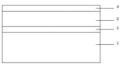
[0014] (1) Deposit the crystalline silicon wafer after cleaning, texturing, diffusion and etching by tubular PECVD to obtain the first layer of high refractive index silicon nitride anti-reflection film. The PECVD parameters are set as: ammonia gas flow rate 6.5slm, silane flow rate 750sccm , pressure 1600mTorr, RF power 7300w, switch time 5:50ms, time 80s;

[0015] (2) Deposit the anti-reflection film obtained after step (1) by tubular PECVD again to obtain the second layer of high-refractive-index silicon nitride anti-reflection film. The PECVD parameters are set to: ammonia gas flow rate 4.8slm, silane flow rate 850sccm, pressure 1600mTorr, RF power 7300w, switch time 5:50ms, time 280s;

[0016] (3) Deposit the anti-reflection film obtained after step (2) by tubular PECVD again to obtain the third layer of low-refractive-index silicon nitride anti-reflection film. The PECVD parameters are set to: ammonia gas flow rate 6.5slm, silane flow rate 650sccm, pressure 1600mTorr, T...

Embodiment 2

[0019] (1) Deposit the crystalline silicon wafer after cleaning, texturing, diffusion and etching by tubular PECVD to obtain the first layer of high refractive index silicon nitride anti-reflection coating. The PECVD parameters are set to: ammonia gas flow rate 7 slm, silane flow rate 800 sccm , pressure 1700mTorr, RF power 7000w, switching time 5:50ms, time 100s;

[0020] (2) Deposit the anti-reflection film obtained after step (1) by tubular PECVD again to obtain the second layer of high-refractive-index silicon nitride anti-reflection film. The PECVD parameters are set to: ammonia gas flow rate 5.2slm, silane flow rate 900sccm, pressure 1700mTorr, RF power 7000w, switch time 5:50ms, time 300s;

[0021] (3) Deposit the anti-reflection film obtained after the completion of step (2) by tubular PECVD again to obtain the third layer of low-refractive index silicon nitride anti-reflection film. The PECVD parameters are set as: ammonia gas flow rate 6.8 slm, silane flow rate 680 s...

Embodiment 3

[0024] (1) Deposit the crystalline silicon wafer after cleaning, texturing, diffusion and etching by tubular PECVD to obtain the first layer of high refractive index silicon nitride anti-reflection film. The PECVD parameters are set as: ammonia gas flow rate 7.2slm, silane flow rate 850sccm , pressure 1800mTorr, RF power 6500w, switching time 5:50ms, time 130s;

[0025] (2) Deposit the anti-reflection film obtained after step (1) by tubular PECVD again to obtain the second layer of high refractive index silicon nitride anti-reflection film. The PECVD parameters are set to: ammonia gas flow rate 5.5slm, silane flow rate 950sccm, pressure 1800mTorr, RF power 6500w, switch time 5:50ms, time 330s;

[0026] (3) Deposit the anti-reflection film obtained after the completion of step (2) by tubular PECVD again to obtain the third layer of low-refractive index silicon nitride anti-reflection film. The PECVD parameters are set to: ammonia gas flow rate 7.5slm, silane flow rate 750sccm, ...


PUM


Abstract

The invention relates to a method for manufacturing a high-refractive-index silicon nitride antireflection film. According to the method, the high-refractive-index silicon nitride antireflection film formed by three silicon nitride antireflection films is obtained by sequentially plating the upper surface, having been subject to cleaning, texturing, diffusion and etching, of a crystalline silicon wafer with one high-refractive-index silicon nitride antireflection film with the refractive index ranging from 2.10 to 2.15, one high-refractive-index silicon nitride antireflection film with the refractive index ranging from 2.25 to 2.30 and another low-refractive-index silicon nitride antireflection film with the refractive index ranging from 2.00 to 2.05, wherein the refractive index of the obtained high-refractive-index silicon nitride antireflection film ranges from 2.12 to 2.16. The high-refractive-index silicon nitride antireflection film manufactured through the method can meet the requirement for PID resistance of a battery assembly; in addition, compared with a traditional process for manufacturing a high-refractive-index antireflection film, the method has the advantages that the conversion rate of the finished product is improved by more than 0.05%, the open-circuit voltage of the finished product is improved by 1mV, and the short-circuit current of the finished product is improved by 30mA or so.

Description

technical field [0001] The invention belongs to the technical field of solar cells, in particular to a method for manufacturing a high-refractive-index silicon nitride anti-reflection film. Background technique [0002] Research in recent years has shown that the high voltage between the circuit in the crystalline silicon photovoltaic module and its grounded metal frame will cause continuous degradation of the photovoltaic performance of the module. There are many mechanisms causing such attenuation. For example, under the action of the above-mentioned high voltage, the ion migration phenomenon that occurs in the packaging material of the component battery and the materials of the upper surface layer and the lower surface layer of the component; sub-phenomena; charge redistribution cuts down on the active layer of the battery; associated circuits are corroded, etc. These mechanisms that cause attenuation are called potential-induced attenuation and polarization (Potential I...

Claims


Application Information

Patent Timeline
IPC IPC(8): H01L31/18H01L31/0216
CPCC23C16/345H01L31/02168Y02P70/50
Inventor 朱金浩
Owner ZHEJIANG GUANGLONG ENERGY TECH
Why Eureka
Try Eureka