Fabrication method of silicon nitride antireflection film on surface of polycrystalline solar cell

A silicon nitride reduction and solar cell technology, applied in the field of solar cells, can solve problems such as poor product stability and simple structure of solar cells, and achieve the effect of increasing the refractive index

Active Publication Date: 2017-04-19
ZHEJIANG GUANGLONG ENERGY TECH
View PDF5 Cites 0 Cited by
  • Summary
  • Abstract
  • Description
  • Claims
  • Application Information

AI Technical Summary

Problems solved by technology

[0004] Although the solar cell disclosed in this patent can make it have better light transmission, the solar cell has a simple structure, is prone to continuous attenuation, and has poor product stability. Therefore, a polycrystalline solar cell surface nitride The fabrication method of silicon anti-reflection coating is very necessary

Method used


Image

  • Fabrication method of silicon nitride antireflection film on surface of polycrystalline solar cell
  • Fabrication method of silicon nitride antireflection film on surface of polycrystalline solar cell
  • Fabrication method of silicon nitride antireflection film on surface of polycrystalline solar cell

Examples


Embodiment Construction

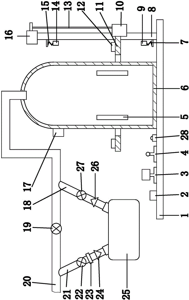
[0052] The following are specific embodiments of the present invention and in conjunction with the accompanying drawings, further describe the technical solution of the present invention, but the present invention is not limited to these embodiments.

[0053] The preparation method of the silicon nitride anti-reflection film on the surface of the polycrystalline solar cell comprises the following steps:

[0054] a. Cleaning, texturing, diffusion and etching of crystalline silicon wafers, treatment of waste gas generated by cleaning texturing and etching through acid mist treatment device, and treatment of exhaust gas generated by diffusion through exhaust treatment device;

[0055] b. Use the crystalline silicon wafer completed in step a to generate a layer of 1-2nm SiO on the surface of the crystalline silicon wafer through an ozone generator 2 Oxide film; in this embodiment, a 1.5nm layer of SiO2 is formed on the surface of the silicon wafer through an ozone generator on the...


PUM

PropertyMeasurementUnit
refractive indexaaaaaaaaaa

Abstract

The invention provides a polycrystalline solar cell surface silicon nitride antireflection film preparation method, which solves the technical problems that an existing solar cell is simple in structure, is easy to have continuous attenuation and is poor in product stability. The polycrystalline solar cell surface silicon nitride antireflection film preparation method comprises the following steps: a) carrying out cleaning, texturing, diffusion and etching on a crystalline silicon wafer; b) enabling the crystalline silicon wafer obtained after the step a) to pass through an ozone generation device to generate a 1-2 mm SiO2 oxidation film on the surface of the silicon wafer; c) cleaning a graphite boat through a cleaning device, placing the crystalline silicon wafer obtained after the step b) on the graphite boat, and placing the graphite boat loaded with the wafer to a tubular PECVD for pre-deposition and cleaning; d) carrying out tubular PECVD deposition on the crystalline silicon wafer obtained in the step c); and e) carrying out tubular PECVD deposition again on the crystalline silicon wafer obtained in the step d). The method has the advantages of stable and reliable product.

Description

technical field [0001] The invention belongs to the technical field of solar cells, and relates to a manufacturing method, in particular to a manufacturing method of a silicon nitride antireflection film on the surface of a polycrystalline solar cell. Background technique [0002] Research in recent years has shown that the high voltage between the circuit in the crystalline silicon photovoltaic module and its grounded metal frame will cause continuous degradation of the photovoltaic performance of the module. There are many mechanisms that cause such attenuation. For example, under the action of the above-mentioned high voltage, the ion migration phenomenon that occurs in the packaging material of the component battery and the materials of the upper surface layer and the lower surface layer of the component; the heat load that occurs in the battery The flow phenomenon; the redistribution of charges reduces the active layer of the battery; the related circuits are corroded, ...

Claims


Application Information

Patent Timeline
Patent Type & Authority Patents(China)
IPC IPC(8): H01L31/0216H01L31/18
CPCH01L31/02168Y02E10/50Y02P70/50
Inventor 朱金浩蒋剑波朱世杰许布万光耀陈珏荣吴振宏文长洪
Owner ZHEJIANG GUANGLONG ENERGY TECH
Why Eureka
Try Eureka