Flip-chip light-emitting diode with symmetrical electrodes and its preparation method

A technology of light-emitting diodes and symmetrical electrodes, applied in circuits, electrical components, semiconductor devices, etc., can solve problems that affect the stability and welding yield of flip-chip light-emitting diodes, P and N-type solder joints are short-circuited, and chips do not emit light. Achieve good soldering contact, improve uniformity, and improve yield

Active Publication Date: 2016-04-13
HC SEMITEK SUZHOU
View PDF4 Cites 0 Cited by
  • Summary
  • Abstract
  • Description
  • Claims
  • Application Information

AI Technical Summary

Problems solved by technology

In the subsequent process of packaging the LED chip, it is necessary to weld the LED chip and the heat-conducting substrate together. During the welding process, due to the large difference in the area of ​​the P-type and N-type solder joints, the stress they receive is different, causing the chip to shift. Cause P, N-type solder joint short circuit, the chip does not emit light, which seriously affects the stability and soldering yield of the packaged flip-chip LED

Method used


Image

  • Flip-chip light-emitting diode with symmetrical electrodes and its preparation method
  • Flip-chip light-emitting diode with symmetrical electrodes and its preparation method
  • Flip-chip light-emitting diode with symmetrical electrodes and its preparation method

Examples


Embodiment 1

[0065] This embodiment provides a method for manufacturing a flip-chip light-emitting diode with symmetrical electrodes. refer to figure 1 , the method includes:

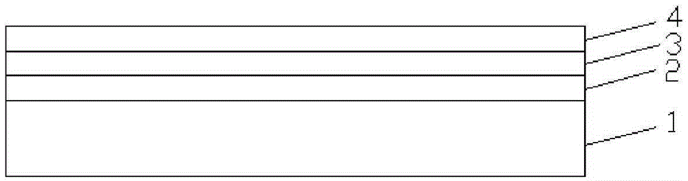
[0066] In step S101, a substrate 1 is provided, and an N-type semiconductor 2, an active region 3 and a P-type semiconductor 4 are sequentially grown up on the substrate 1 (see Picture 1-1 );

[0067] In this embodiment, the substrate 1 may be a substrate formed of any one of sapphire, diamond, silicon and gallium arsenide. It can be understood that the growth of the N-type semiconductor 2 , the active region 3 and the P-type semiconductor 4 can be realized by vapor deposition by MOCVD (Metal-organic Chemical Vapor Deposition) equipment.

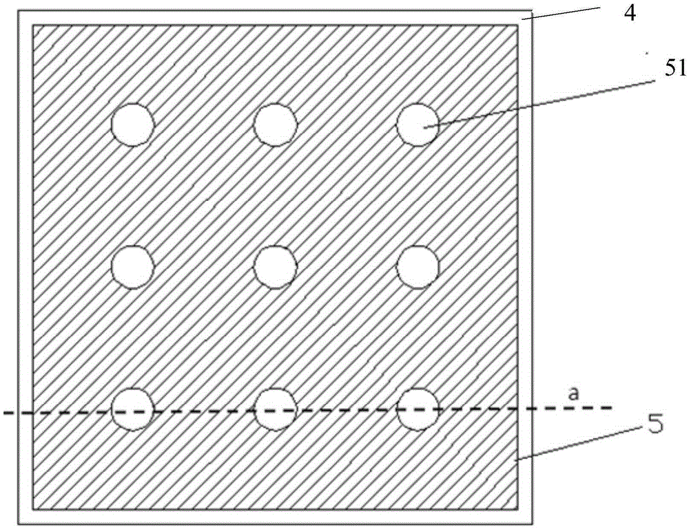
[0068] Step S102, preparing a reflective layer 5 on the P-type semiconductor 4 (see diagram 2-1 with Figure 2-2 );

[0069] It should be noted that the reflective layer 5 may be a film with high reflectivity and high conductivity. The reflective layer 5 is located on the...

Embodiment 2

[0108] This embodiment provides a flip-chip light emitting diode with symmetrical electrodes. see Figure 10-2 with Figure 10-3 , the flip-chip LED consists of:

[0109] Substrate 1, N-type semiconductor 2, active region 3, P-type semiconductor 4, light-reflecting layer 5 and electrode protection layer 6 grown upwards on the substrate 1 in sequence, and a plurality of first small holes are opened on the light-reflecting layer 5 51, the first small hole 51 extends from the reflective layer 5 to the P-type semiconductor (see diagram 2-1 with Figure 2-2 );

[0110] The electrode protection layer 6 covers the exposed surface (i.e. the upper surface and the side wall) of the reflective layer 5, and the electrode protection layer 6 is provided with a plurality of second small holes 61, and the second small holes 61 are connected with the first small holes 51. Correspondingly arranged, the second small hole 61 extends from the electrode protection layer 6 to the N-type semico...


PUM

PropertyMeasurementUnit
melting pointaaaaaaaaaa
thicknessaaaaaaaaaa
thicknessaaaaaaaaaa

Abstract

The invention discloses a flip-chip light emitting diode with symmetrical electrodes, and a preparation method thereof, and relates to the technical field of a semiconductor. The method comprises the following steps: growing an N-type semiconductor, an active area and a P-type semiconductor; preparing a reflection layer; arranging a first small hole in the reflection layer; preparing an electrode protection layer; arranging a second small hole in the electrode protection layer; preparing a first passivation layer; arranging a third small hole and a fourth small hole in the first passivation layer; preparing a first layer N electrode and a first layer P electrode; preparing a second passivation layer; preparing a fifth small hole and a sixth small hole in the second passivation layer; and preparing a second layer N electrode (i.e., N-type welding point) and a second layer P electrode (i.e., P-type welding point) which have equal areas and are symmetrically distributed. According to the invention, the N-type welding point and the P-type welding point which have equal areas and are symmetrically distributed can be prepared, a chip is not displaced during a process of welding a flip-chip light emitting diode with a heat conduction substrate, and a flip-chip device with food welding contact and reliable connection can be obtained.

Description

technical field [0001] The invention relates to the technical field of semiconductors, in particular to a flip-chip light-emitting diode with symmetrical electrodes and a preparation method thereof. Background technique [0002] With the progress of material growth technology and device structure design and production, the preparation and wire bonding technology of front-mounted light-emitting diodes are quite mature, but they are affected by GaN material absorption, electrode absorption, the critical angle of total reflection between GaN material and air interface, and thermal resistance. Influenced by factors such as large ones, the light extraction efficiency of LEDs (Light Emitting Diodes, light-emitting diodes) with traditional front-mounted structures (hereinafter referred to as front-mounted LEDs) is very low. In recent years, another device structure has emerged, that is, LEDs with a flip-chip structure (hereinafter referred to as flip-chip LEDs for short). Compared...

Claims


Application Information

Patent Timeline
Patent Type & Authority Patents(China)
IPC IPC(8): H01L33/38H01L33/40H01L33/00
CPCH01L33/0075H01L33/387H01L33/44
Inventor 杨春艳徐瑾王江波
Owner HC SEMITEK SUZHOU
Why Eureka
Try Eureka