Cellular structure of silicon carbide VDMOS device and manufacturing method thereof

A technology of silicon carbide and devices, which is applied in the field of power semiconductor devices, can solve the problems of increasing the on-state resistance of the JFET area and reducing the dV/dt ability, and achieve the effects of improving the conduction ability, not being easy to open, and improving reliability

Active Publication Date: 2020-05-12
湖南国芯半导体科技有限公司
View PDF4 Cites 4 Cited by
  • Summary
  • Abstract
  • Description
  • Claims
  • Application Information

AI Technical Summary

Problems solved by technology

[0006] Due to the dV of the SiC MOSFET D / dt is higher, and the concentration of the P+ shielding area is higher, which will lead to the capacitance C of the junction of the P+ shielding area / N drift area DB increases when there is an extremely high dV of the drain D / dt, the current I D C via the drain to the P+ shield DB Flow, I D =C DB [dV D / dt], C DB Big cause I D increase, it is easy to cause the forward bias of the source N+ / P base junction, which leads to the opening of the parasitic NPN transistor and reduces the dV / dt capability; and the existence of the P+ shielding area will further bring about the JFET bottleneck area, resulting in the JFET area on-state resistance Ron( JFET) increase

Method used


Image

  • Cellular structure of silicon carbide VDMOS device and manufacturing method thereof
  • Cellular structure of silicon carbide VDMOS device and manufacturing method thereof
  • Cellular structure of silicon carbide VDMOS device and manufacturing method thereof

Examples


no. 1 example

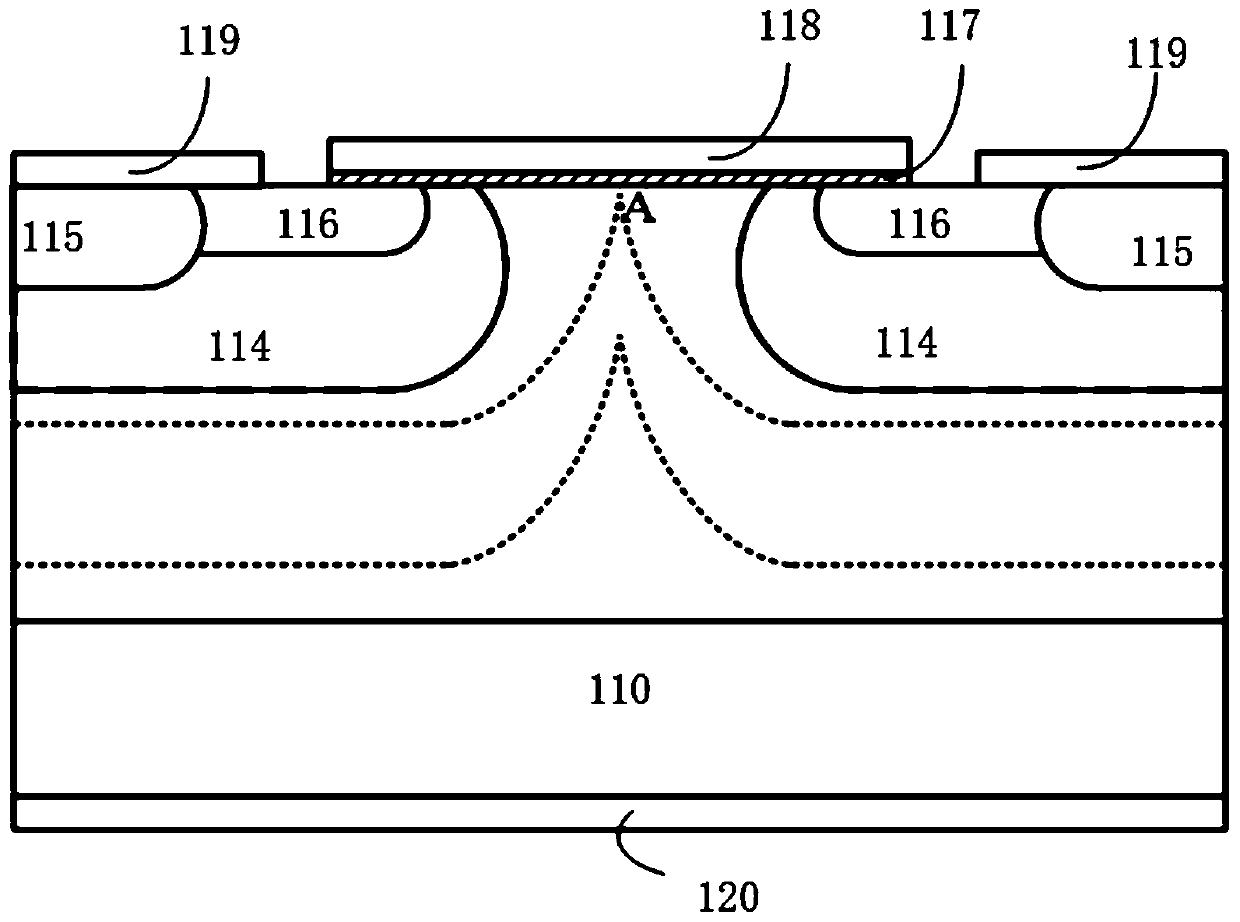
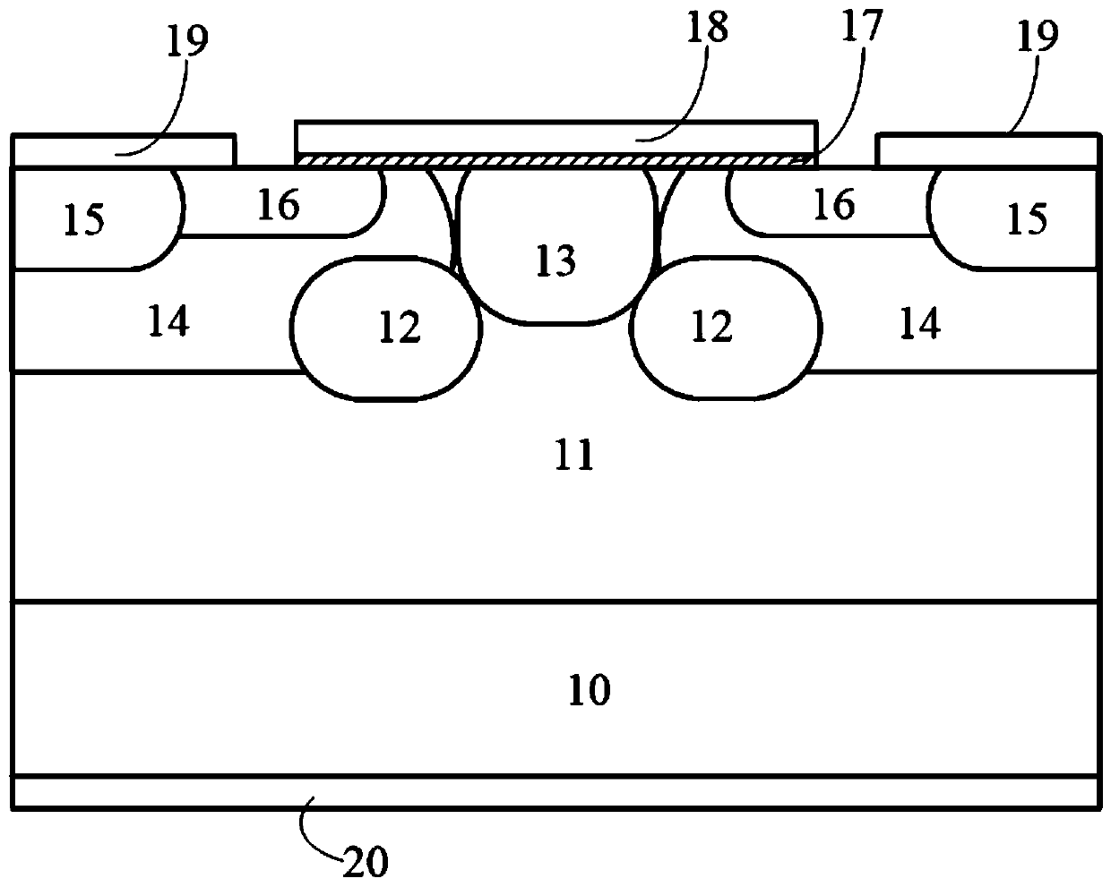
[0086] image 3 It is a schematic diagram of a cross-sectional structure of a silicon carbide VDMOSFET in this embodiment,

[0087] Figure 4 It is a schematic diagram of the electric field when the silicon carbide VDMOSFET is turned off in this embodiment.

[0088] The cell structure of a silicon carbide VDMOS device provided by this implementation, such as image 3 ,include:

[0089] The first conductivity type substrate 10, the first conductivity type drift region 11, the second conductivity type shielding region 12, the first conductivity type JFET injection region 13, the second conductivity type base region 14, the second conductivity type source region 15, the second conductivity type One conductivity type source region 16 , gate insulating layer 17 , gate 18 , source electrode 19 , drain electrode 20 .

[0090] When the SiC VDMOSFET is turned off, the electric field as Figure 4 , wherein the electric field distribution in the drift region 11 of the first conducti...

no. 2 example

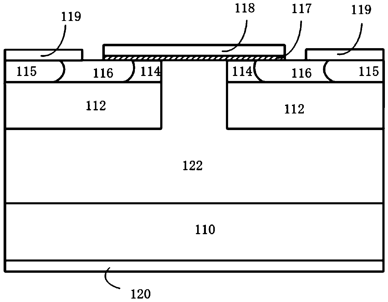
[0112] Figure 5 It is a schematic diagram of a cross-sectional structure of a silicon carbide VDMOSFET in this embodiment,

[0113] Figure 6 It is a schematic diagram of the electric field when the silicon carbide VDMOSFET is turned off in this embodiment.

[0114] The cell structure of a silicon carbide VDMOS device provided by this implementation, such as Figure 5 ,include:

[0115] The first conductivity type substrate 10, the first conductivity type drift region 11, the second conductivity type shielding region 12, the first conductivity type JFET injection region 13, the first conductivity type epitaxial region 21, the second conductivity type base region 14, the second conductivity type The second conductivity type source region 15 , the first conductivity type source region 16 , the gate insulating layer 17 , the gate 18 , the source electrode 19 , and the drain electrode 20 .

[0116] When the SiC VDMOSFET is turned off, the electric field as Figure 6 , wherei...

no. 3 example

[0140] Figure 7 It is a schematic flow chart of the fabrication method of the cell structure of the silicon carbide VDMOS device in this embodiment.

[0141] The present invention also provides a method for making a cell structure of a silicon carbide VDMOS device, the specific process is as follows Figure 7 , including the following steps:

[0142] S310, growing the drift region 11 of the first conductivity type on the substrate 10 of the first conductivity type, such as Figure 7.1 ;

[0143] Then form several shielding regions 12 of the second conductivity type, JFET injection regions 13 of the first conductivity type, base regions 14 of the second conductivity type, source regions 16 of the first conductivity type and source regions 15 of the second conductivity type, specifically,

[0144] S320, forming the shielding region 12 of the second conductivity type at a specified depth by implanting ions into the surface of the drift region 11 of the first conductivity type...


PUM

PropertyMeasurementUnit
thicknessaaaaaaaaaa
electrical resistivityaaaaaaaaaa

Abstract

The invention discloses a cellular structure of a silicon carbide VDMOS device and a manufacturing method thereof. A first conductive type drift region is arranged on a first conductive type substrate, a gate insulating layer and a gate arranged on the insulating layer are arranged on the surface of the cellular structure, a first conductive type JFET injection region is arranged downwards on thesurface of the first conductive type drift region at the central part, and a plurality of gate structures which are symmetrically distributed are arranged on the edge part of the cellular structure and the surface of the first conductive type drift region. The coverage area of the second conductive type shielding region is reduced, a first conductive type JFET injection region is newly arranged inthe JFET region, the first conductive type epitaxial region can be further arranged, the capacitance CDB of the junction of the second conductive type shielding region/the first conductive type driftregion is reduced, the starting probability of a parasitic NPN tube is reduced, the capability of dV/dt is not reduced, the reliability of the device is improved, the on-state resistance of the JFETregion is reduced by improving the concentration of the JFET region, and the conduction capability of the device is greatly improved.

Description

technical field [0001] The invention relates to the technical field of power semiconductor devices, in particular to a cell structure of a silicon carbide VDMOS device and a manufacturing method thereof. Background technique [0002] Silicon carbide (SiC) is a new type of wide-bandgap semiconductor material with excellent physical, chemical and electrical properties. The breakdown electric field strength of silicon carbide is 10 times that of traditional silicon, and the thermal conductivity is 3 times that of silicon. This makes silicon carbide very attractive and promising in power semiconductor devices, especially in high-power and high-temperature applications. [0003] At present, the domestic economic model has changed from the development and use of resources to the effective utilization of resources. In today's energy saving and emission reduction, silicon carbide devices with high conversion efficiency have great potential to contribute to power electronics applicat...

Claims


Application Information

Patent Timeline
Patent Type & Authority Applications(China)
IPC IPC(8): H01L29/78H01L29/06H01L23/552H01L21/336
CPCH01L29/7802H01L29/0607H01L23/552H01L29/66068Y02B70/10
Inventor 高秀秀李诚瞻齐放戴小平
Owner 湖南国芯半导体科技有限公司
Why Eureka
Try Eureka