

High-speed junction field effect transistor used in bipolar integrated circuit
A technology of field effect transistors and integrated circuits, applied in the field of high-speed junction field effect transistors, can solve problems affecting device degradation and hysteresis
- Summary
- Abstract
- Description
- Claims
- Application Information
AI Technical Summary
Problems solved by technology
Method used
Image

Examples
Embodiment Construction
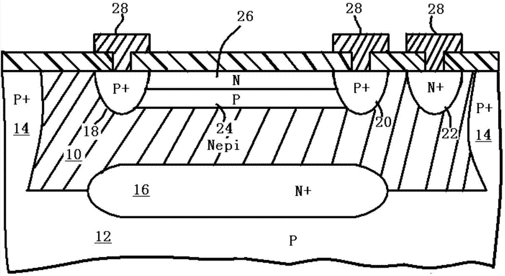
[0014] figure 1 and figure 2 is a cross-sectional view of a prior art bipolar field effect transistor device. according to figure 1 , an N-type epitaxial layer 10 is formed on the surface of a P-type silicon substrate 12 , and the device region is defined by a P+ isolation diffusion ring 14 . An N+ buried layer 16 is formed by doping the surface region of the substrate 12 of the epitaxially grown layer 10 . A bipolar field effect transistor is formed on the epitaxial layer 10 having a source region 18 and an empty drain region 20 formed by diffused dopant ions P+. One gate contact 22 is formed by diffused dopant ions N+. A P-type channel 24 is formed by ion implantation between the source and gate regions 18 , 20 and a lightly doped top gate layer 26 is formed by ion implantation on the surface of the source and drain regions. The N-type top gate layer 26 is associated with the bottom gate contact defined by the epitaxial layer 10 by the epitaxial structure. Metal conta...
PUM
 Abstract
Description
Claims
Application Information