Double-mode electro-static discharge protection IO circuit

A technology for electrostatic discharge protection and circuit protection. It is applied in the direction of static electricity, circuits, and electrical components. It can solve problems such as breakdown failure, electrostatic discharge damage, and device electrostatic breakdown failure.

Active Publication Date: 2014-03-19
BEIJING CEC HUADA ELECTRONIC DESIGN CO LTD
View PDF3 Cites 8 Cited by
  • Summary
  • Abstract
  • Description
  • Claims
  • Application Information

AI Technical Summary

Problems solved by technology

Therefore, the NMOS and PMOS directly connected to the I / O PAD in the core circuit are very prone to electrostatic discharge damage.
When the ESD current flows through these devices, these devices are equivalent to a certain on-resistance, so a certain voltage difference will be formed along the ESD path, if the voltage difference between two nodes exceeds the breakdown of the devices connected to the nodes voltage, will cause breakdown failure
For example, in the nanometer process, the breakdown voltage of the core device may be lower than 10V. If the voltage difference formed by the ESD current at both ends of the core device exceeds 10V, it will cause the device to fail due to electrostatic breakdown.
[0005] Due to the large difference in the discharge current of the HBM and E-Gun models, taking the minimum protection requirement of 2000V electrostatic level in the industry as an example, the discharge current of the HBM model is about 1.33A, while the discharge current of the E-Gun model is about 6.5A, which also flows through a When turning on a device with a resistance of 2ohm, under HBM, the generated voltage difference is about 2.7V, which is far lower than the breakdown voltage of the device. The core circuit is relatively safe, but under the E-Gun model, the generated voltage difference is about 13V, which is already If the breakdown voltage of some devices is exceeded, the device will be broken down, and the circuit will fail in ESD

Method used


Image

  • Double-mode electro-static discharge protection IO circuit
  • Double-mode electro-static discharge protection IO circuit
  • Double-mode electro-static discharge protection IO circuit

Examples


Embodiment Construction

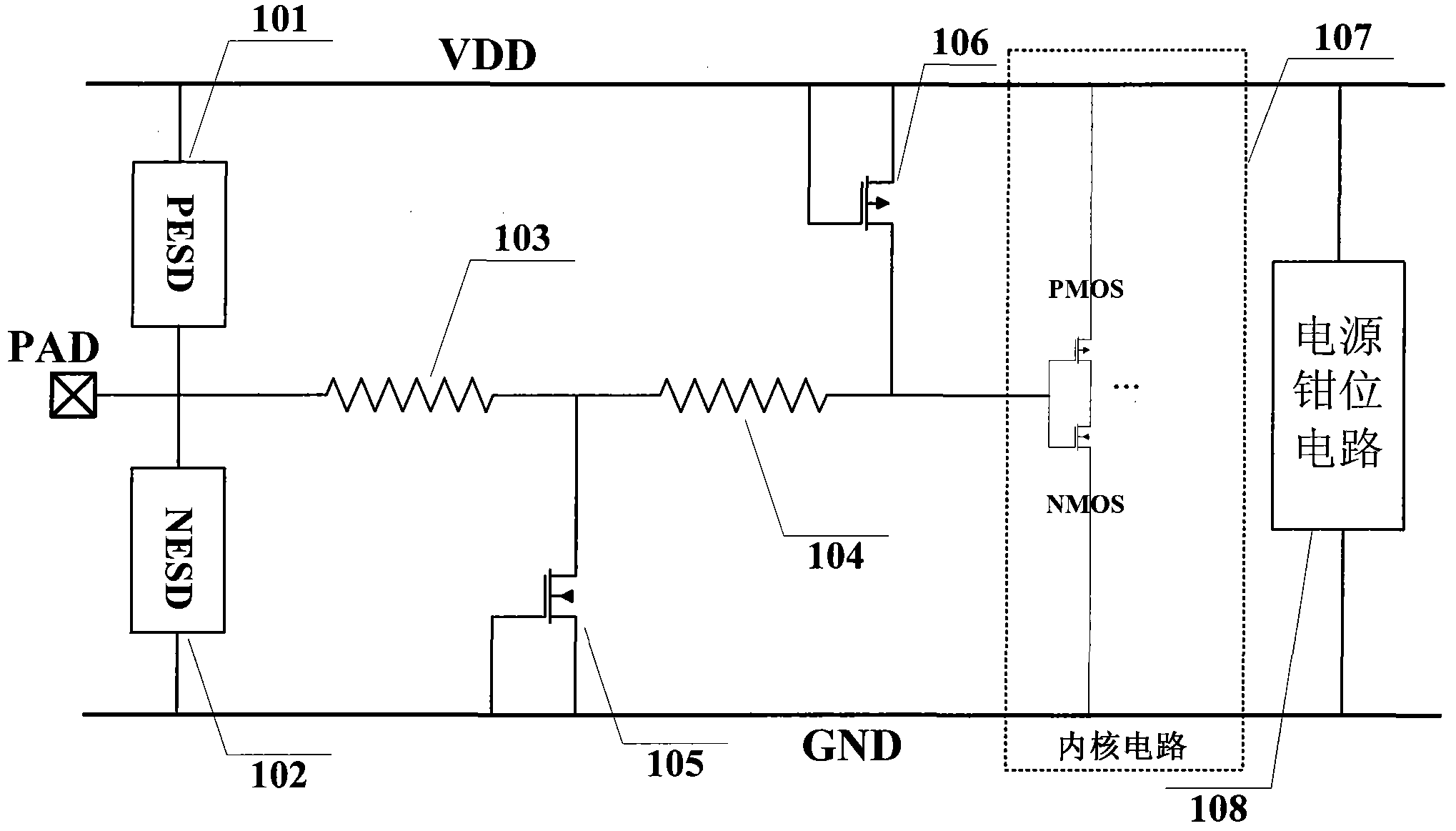
[0014] The present invention is a dual-mode electrostatic discharge protection I / O circuit, which can not only realize the protection of HBM discharge, but also provide protection for E-Gun model discharge. The implementation plan is as follows:

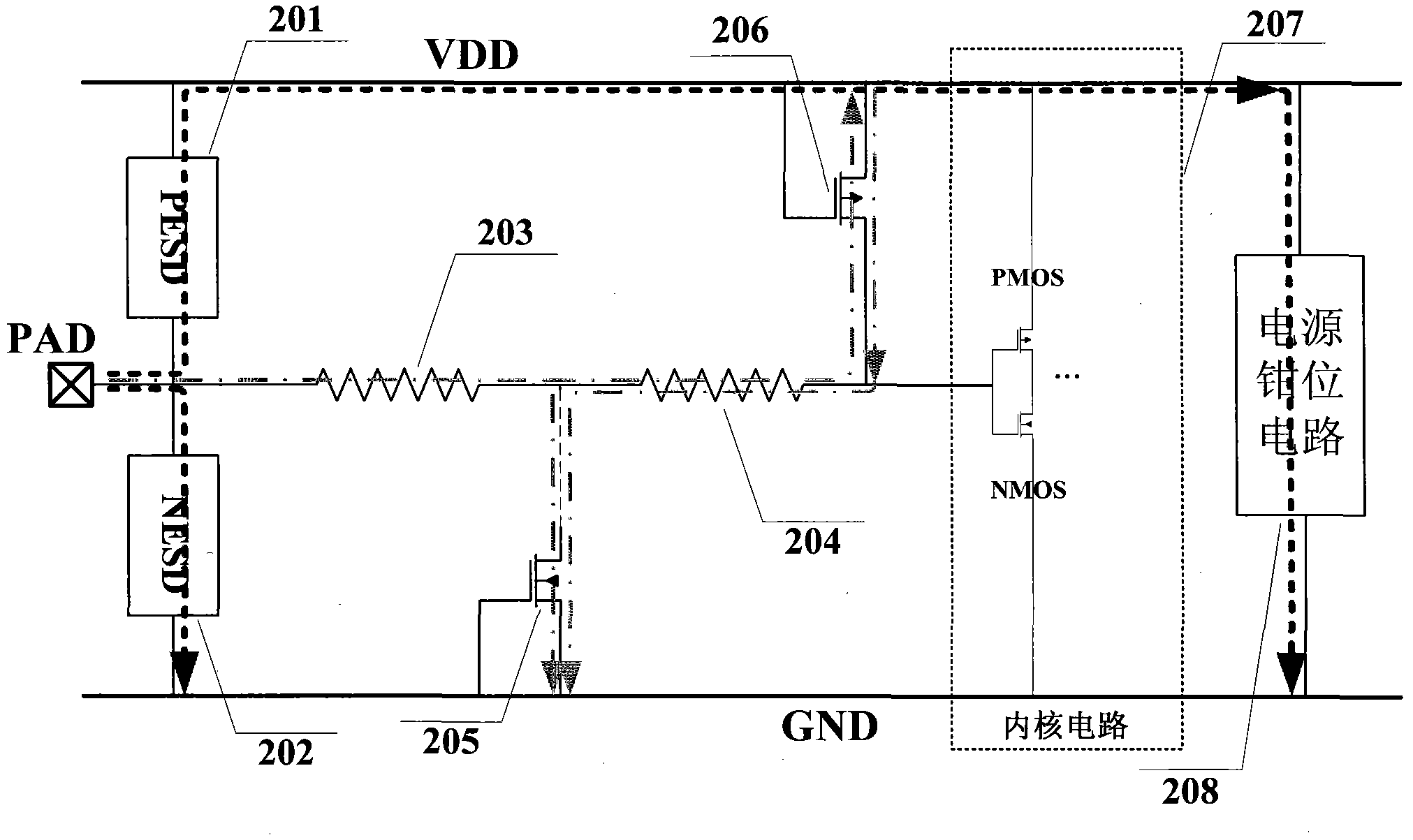
[0015] like figure 2 , is the discharge path when the I / O circuit E-Gun model of the present invention discharges. Take I / O-GND forward 2000V electrostatic discharge as an example, at this time, GND is grounded, and positive charge electrostatic discharge is performed on I / O PAD.

[0016] First, the NESD202 of the primary protection will be turned on and discharged, forming a figure 2 The high-current discharge path from PAD to GND through 202 is one of the main electrostatic discharge paths. At this time, the voltage at the PAD terminal will exceed 10V, so the secondary protection NMOS205 will also be turned on, clamping the core circuit to GND at a safe level, and at the same time, due to the function of the input protection re...


PUM


Abstract

The invention relates to the technical field of integrated circuit (IC: Integrated Circuit) electro-static discharge (ESD: Electro-Static Discharge) protection design in microelectronics and discloses a double-mode ESD protection I / O (Input / Output) circuit. The double-mode ESD protection I / O circuit is characterized in that a first-level protection circuit and a second-level protection circuit are collaboratively designed, an ESD high-current discharge path is provided, and meanwhile, comprehensive protection on a core circuit is realized through a bidirectional voltage clamp protection technology and protection on the ESD circuit is realized through a current limiting protection technology. The double-mode electro-static discharge protection I / O circuit of the invention can provide a targeted discharge path and targeted protection respectively for the two different discharge patterns: human body model discharge and electron gun model discharge.

Description

technical field [0001] The invention relates to a dual-mode electrostatic discharge protection I / O circuit, which is suitable for the design of electrostatic discharge protection of integrated circuits, and is especially suitable for the dual-mode electrostatic discharge protection design of a human body discharge model and an electron gun discharge model. Background technique [0002] As the level of integrated circuit manufacturing technology has entered the deep submicron era and nanometer era, the MOS transistors in the integrated circuit all adopt the lightly doped structure LDD (Lightly Doped Drain); the silicide is covered on the diffusion area of ​​the MOS transistor; the polycrystalline compound process It is used to reduce the series resistance of the gate polysilicon; and the thickness of the gate oxide layer of the MOS transistor is getting thinner and the channel length is getting smaller and smaller. These improvements have improved the integration of the chip,...

Claims


Application Information

Patent Timeline
Patent Type & Authority Applications(China)
IPC IPC(8): H01L27/02H05F3/00H03K19/003
Inventor 李志国孙磊
Owner BEIJING CEC HUADA ELECTRONIC DESIGN CO LTD
Why Eureka
Try Eureka