Method for preparing and applying single orientation Cu6Sn5 intermetallic compound micro-interconnecting welding point structure

An intermetallic compound, solder joint technology, applied in metal processing equipment, welding equipment, metal processing and other directions, can solve the problems of high cost, complex process, unsuitable for large-scale production, etc., to achieve low cost, simple process, avoid premature Ineffective effect

Active Publication Date: 2014-03-26
HARBIN INST OF TECH SHENZHEN GRADUATE SCHOOL +3
View PDF6 Cites 44 Cited by
  • Summary
  • Abstract
  • Description
  • Claims
  • Application Information

AI Technical Summary

Problems solved by technology

However, this method requires a large number of improvements to the existing mature electroplating process and equipment, the process is complicated, the cost is high, and it is not suitable for large-scale production.

Method used


Image

  • Method for preparing and applying single orientation Cu6Sn5 intermetallic compound micro-interconnecting welding point structure
  • Method for preparing and applying single orientation Cu6Sn5 intermetallic compound micro-interconnecting welding point structure
  • Method for preparing and applying single orientation Cu6Sn5 intermetallic compound micro-interconnecting welding point structure

Examples


Embodiment 1

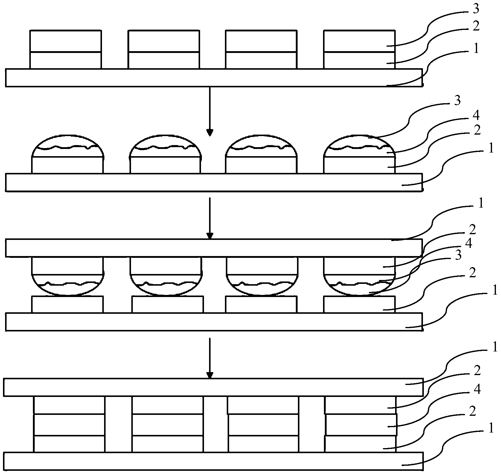
[0036] Such as figure 1 As shown, 1 is the silicon wafer (or PCB board), 2 is the Cu metallurgical pad, 3 is the solder, and 4 is the interface Cu6Sn5 intermetallic compound.

[0037] (1) 8×8 Cu pads with a diameter of 200 μm and a thickness of 36 μm are arrayed on the wafer by electroplating process;

[0038] (2) Prepare a 50 μm thick solder on the Cu pad prepared in step (1) by electroplating process, and the solder composition is Sn3.5Ag eutectic solder

[0039] (3) Perform hot air remelting on the boss prepared in step (2), the remelting temperature is 230°C, and the remelting time is 60s.

[0040] (4) Perform solid-phase aging treatment on the chip prepared in step (3), the solid-phase aging temperature is 150°C, and the aging time is 36 days.

[0041] (5) Put the solder joint boss prepared in step (4) into a 5% hydrochloric acid alcohol solution for 1 min, and then dry it.

[0042] (6) The solder joint boss prepared in step (5) is buckled upside down on the correspond...

Embodiment 2

[0044] (1) An 8×8 Cu metal layer with a diameter of 200 μm and a thickness of 36 μm is arrayed on the wafer by electroplating process;

[0045] (2) Prepare a 50 μm thick solder on the Cu metal layer prepared in step (1) by electroplating process, and the solder composition is Sn37Pb eutectic solder

[0046] (3) Perform hot air remelting on the boss prepared in step (2), the remelting temperature is 200°C, and the remelting time is 60s.

[0047] (4) Perform solid-phase aging treatment on the chip prepared in step (3), the solid-phase aging temperature is 120°C, and the aging time is 36 days.

[0048] (5) Ultrasonically clean the solder joint boss prepared in step (4) in 5% hydrochloric acid alcohol solution for 1 min, and then dry it.

[0049] (6) The solder joint boss prepared in step (5) is buckled upside down on the corresponding Cu pad of the circuit board, and reflowed at 240°C for 120s to obtain a single-oriented Cu6Sn5 intermetallic compound micro-interconnection solder...

Embodiment 3

[0051] (1) 8×8 Cu pads with a diameter of 200 μm and a thickness of 36 μm are arrayed on the wafer by electroplating process;

[0052] (2) Prepare a 50 μm thick solder on the Cu pad prepared in step (1) by electroplating process, and the solder composition is Sn3.5Ag eutectic solder

[0053] (3) Perform hot air remelting on the boss prepared in step (2), the remelting temperature is 230°C, and the remelting time is 120min.

[0054] (4) Put the solder joint boss prepared in step (3) into 3% hydrochloric acid alcohol solution for 1 min, and then dry it.

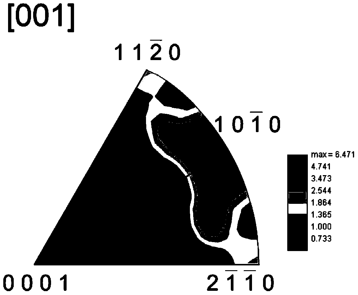
[0055] (5) Upside down the solder bumps prepared in step (4) on the corresponding Cu pads of the circuit board, and reflow at 240°C for 120s to obtain a single-oriented Cu6Sn5 intermetallic compound micro-interconnection solder joint structure such as image 3 As shown (EBSD orientation diagram of the longitudinal section of the solder joint), the orientation of the Cu6Sn5 intermetallic compound in the solder joint presents an o...


PUM

PropertyMeasurementUnit
diameteraaaaaaaaaa
thicknessaaaaaaaaaa

Abstract

The invention provides a method for preparing and applying a single orientation Cu6Sn5 intermetallic compound micro-interconnecting welding point structure. The method for preparing the single orientation Cu6Sn5 intermetallic compound micro-interconnecting welding point structure comprises the first step of arraying a Cu welding disc on a wafer through the electroplating technology, the second step of manufacturing bosses by preparing brazing filler metal prepared on the Cu welding disc, the third step of carrying out hot-wind remelting on the manufactured bosses for 30s-120s, the fourth step of carrying out solid-phase aging processes on chips obtained in the third step, the fifth step of placing the welding point bosses prepared in the fourth step into hydrochloric acid, oscillating the welding point bosses through ultrasound, washing and drying the welding point bosses to obtain a preferred orientation Cu6Sn5 welding disc, the sixth step of reversely buckling the welding point bosses prepared in the fifth step into a corresponding circuit board Cu metal layer, and obtaining the single orientation Cu6Sn5 intermetallic compound micro-interconnecting welding point structure through the reflow welding technology. Uniform and stable welding point structure can be obtained when the single orientation Cu6Sn5 intermetallic compound micro-interconnecting welding point structure is applied to large two-level packaging at the appropriate conditions.

Description

technical field [0001] The invention relates to a preparation and application method of a single-orientation Cu6Sn5 intermetallic compound micro-interconnect solder spot structure. Background technique [0002] Nowadays, the production of microelectronics industry is facing the transition from 2D packaging to 3D packaging. The integration of chips is getting higher and higher, and the size of solder joints in chips is further reduced. At present, the diameter of the solder joint on the flip chip has been reduced to 100 μm, and with the development of through-silicon via technology, this size will be further reduced. Restricted by the melting point of the solder, the interconnection temperature of the chip will not decrease. For such a small solder joint, there will only be a small amount of grains in it after the interconnection is completed, and the interface intermetallic compound will occupy a large proportion. During the service or storage of electronic devices, the sol...

Claims


Application Information

Patent Timeline
Patent Type & Authority Applications(China)
IPC IPC(8): B23K1/00B23K1/20B23K35/26H01L21/60
CPCB23K1/012B23K1/20B23K1/206B23K35/262B23K2101/36H01L21/4825H01L24/81H01L2224/81359
Inventor 李明雨杨明马鑫陈宏涛张志昊
Owner HARBIN INST OF TECH SHENZHEN GRADUATE SCHOOL
Why Eureka
Try Eureka