Integrated photonic quantum walking device based on photonic crystal self-collimation effect

A technology of photonic crystal and light quantum, which is applied in the field of integrated light quantum walking devices, can solve the problems of unfavorable integration, and achieve the effects of avoiding short coupling distance, high coupling efficiency and flexible layout

Active Publication Date: 2016-02-24
INST OF SEMICONDUCTORS - CHINESE ACAD OF SCI
View PDF8 Cites 0 Cited by
  • Summary
  • Abstract
  • Description
  • Claims
  • Application Information

AI Technical Summary

Problems solved by technology

[0005] Existing integrated optical quantum devices are based on ordinary waveguide structures, and the general size is on the order of millimeters or hundreds of microns, which is not conducive to integration

Method used


Image

  • Integrated photonic quantum walking device based on photonic crystal self-collimation effect
  • Integrated photonic quantum walking device based on photonic crystal self-collimation effect
  • Integrated photonic quantum walking device based on photonic crystal self-collimation effect

Examples


Embodiment Construction

[0024] In order to make the object, technical solution and advantages of the present invention clearer, the present invention will be described in further detail below in conjunction with specific embodiments and with reference to the accompanying drawings.

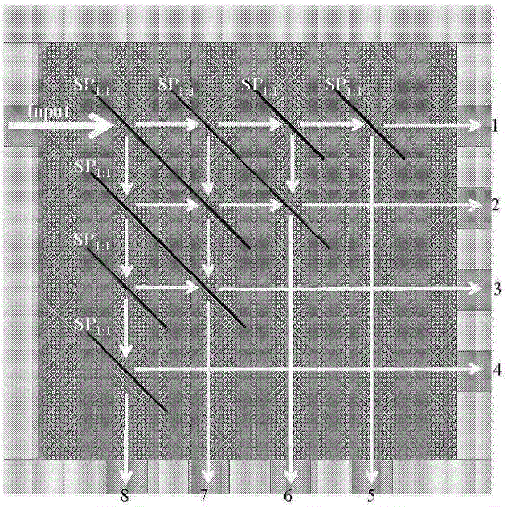
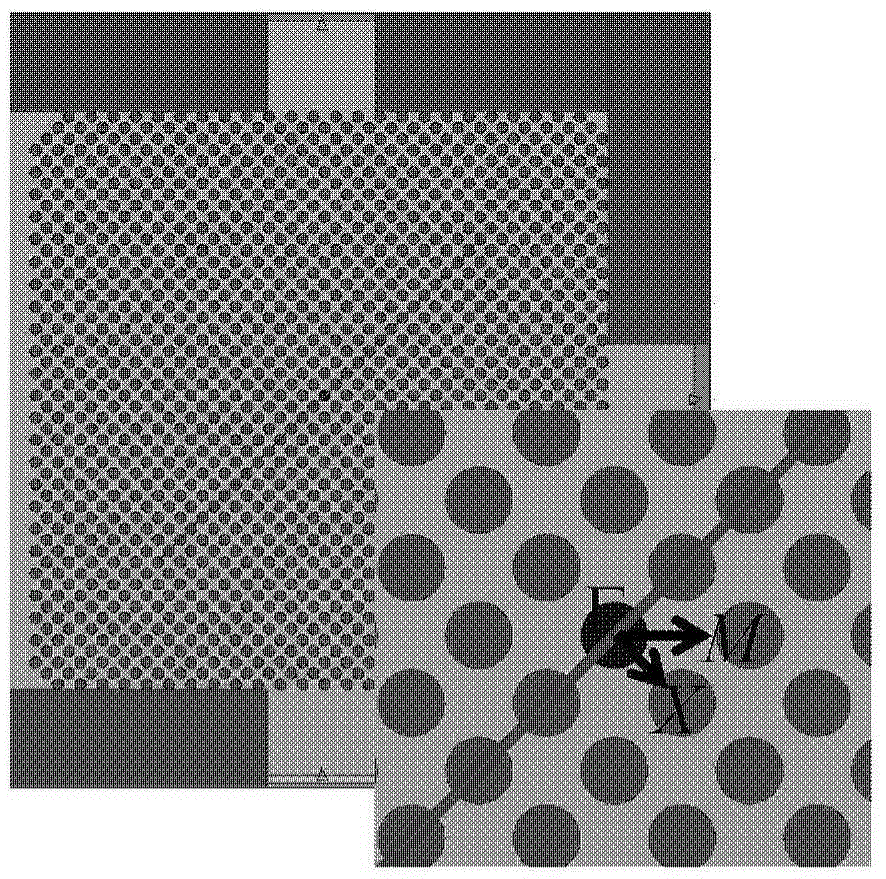
[0025] figure 1 The self-collimation walking device based on the beam splitter array proposed by the present invention and applicable to light quantum walking is shown. Based on the energy band structure and equifrequency lines of tetragonal lattice air holes or dielectric pillar photonic crystals, the first (or second) energy band is taken, since the light is self-collimated and transmitted along the Γ-M (or Γ-X) direction, then Build a beam splitter along the Γ-X (or Γ-M) direction, arrange the beam splitter along the Γ-M (or Γ-X) direction, so that every time the light passes through a fixed transmission distance, that is, every step, along the Γ A beam splitter node in the -X (or Γ-M) direction is added to provide a ...


PUM


Abstract

The invention discloses an integratable light quantum walking device based on the photonic crystal auto-collimation effect. Tetragonal lattice air holes or an energy band structure and an equi-frequency line of a dielectric cylinder photonic crystal are utilized, a first or a second energy band is taken to establish beam splitters in the Gamma-X or Gamma-M direction and arrange the beam splitters in the Gamma-M or Gamma-X direction, wherein beam splitter nodes in the Gamma-X or Gamma-M direction are increased at intervals of fixed transmission distances. The integratable light quantum walking device utilizes the advantages that auto-collimation light beams in the photonic crystal do not diverge during transmission and are free of crosstalk when being crossed, adopts a 3dB beam splitter array to form a micronanoelectronic device capable of being used for light quantum walking and belongs to the fields of semiconductor integrated optical technologies and quantum information science.

Description

technical field [0001] The invention relates to the fields of semiconductor integrated optics technology and quantum information science, in particular to an integrated optical quantum walking device based on the photonic crystal self-collimation effect. Background technique [0002] The development of microelectronics technology has always followed Moore's Law, but according to the semiconductor technology roadmap released by the International Semiconductor Technology Roadmap (ITRS) in 2009, the line width of the world's integrated circuit flash memory will be reduced to 6.3nm by 2024, which is close to the theoretical limit . At that time, microelectronics technology, which uses electrons as information carriers, will encounter theoretical and technical bottlenecks in its development, and it will be difficult to continue to follow Moore's Law for development. Compared with electrons, photons have great advantages as information carriers: photons have no rest mass, there i...

Claims


Application Information

Patent Timeline
Patent Type & Authority Patents(China)
IPC IPC(8): G02B6/122
Inventor 郑婉华王宇飞冯志刚祁帆
Owner INST OF SEMICONDUCTORS - CHINESE ACAD OF SCI
Why Eureka
Try Eureka