

Self-Aligned Dual Patterning Method
A dual-patterning, self-aligning technology, applied in electrical components, semiconductor/solid-state device manufacturing, circuits, etc., can solve the problems of complex process, poor sidewall morphology of etched patterns, etc., and achieve the effect of reducing process steps
- Summary
- Abstract
- Description
- Claims
- Application Information
AI Technical Summary
Problems solved by technology
Method used
Image

Examples
Embodiment Construction
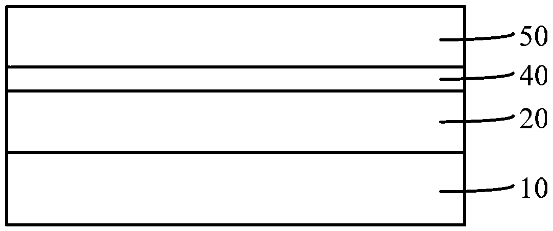
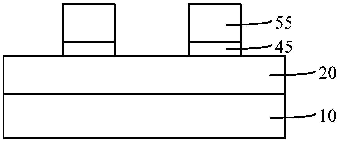
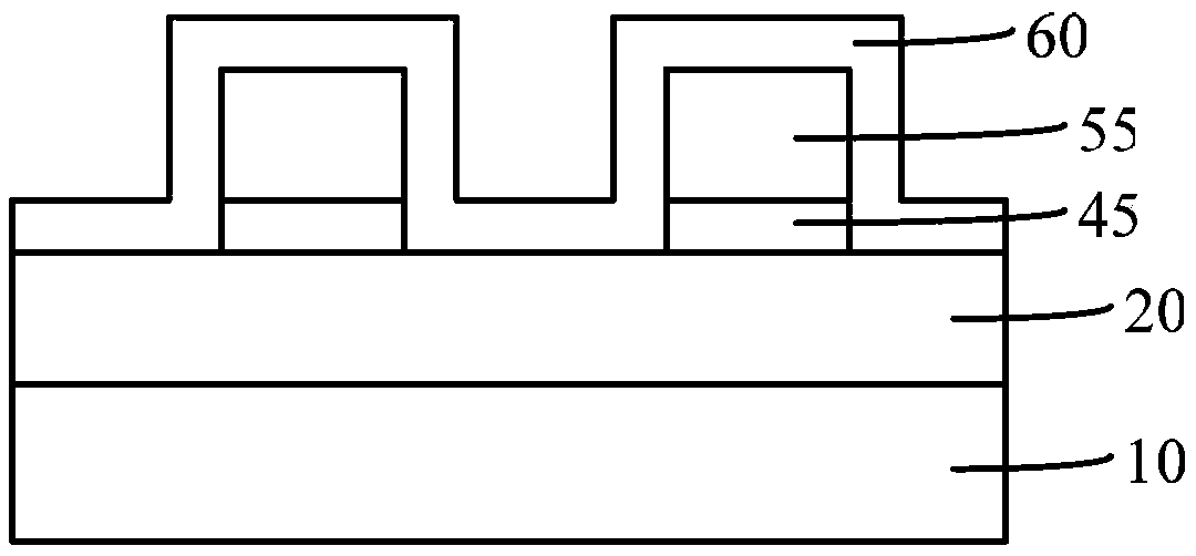
[0035] Due to the poor sidewall morphology of the etched pattern formed by etching the material layer to be etched using the above technology, and the process is complicated, the inventor found through research that when the surface of the sacrificial material layer and the sacrificial photoresist layer is formed with hard When the mask layer is used, the hard mask layer will exert stress on the sacrificial photoresist layer. Since the hardness of the photoresist layer is not large, the sacrificial photoresist layer is relatively soft even after exposure and baking. The stress generated by the hard mask layer will deform the sacrificial photoresist layer, forming a trapezoid-like cross-section. sacrificing the photoresist layer, so that the sidewall of the sacrificial photoresist layer is not perpendicular to the surface of the material layer to be etched, so that the sidewalls formed on the sidewall surface of the sacrificial photoresist layer are not perpendicular to the mate...
PUM
 Abstract
Description
Claims
Application Information