A kind of manufacturing method of split gate mosfet

A fabrication method and separation gate technology, applied in semiconductor/solid-state device manufacturing, semiconductor devices, electrical components, etc., can solve the problems of poor insulation, poor source and gate insulation, large overlapping area, etc., and achieve the reduction of precision requirements. Effect

Active Publication Date: 2022-08-09
捷捷微电(南通)科技有限公司
View PDF4 Cites 0 Cited by
  • Summary
  • Abstract
  • Description
  • Claims
  • Application Information

AI Technical Summary

Problems solved by technology

[0005] 1. Poor insulation of the polysilicon isolation oxide layer (IPO, inter-poly oxide) between the source and the gate leads to an increase in gate-source leakage current Igss;
[0006] 2. The overlapping area between the source and the gate is too large, and the thickness of the isolation oxide layer between polysilicon is insufficient, resulting in a substantial increase in the capacitance Cgs between the source and the gate
[0007] The main reason that causes the above-mentioned shortcoming is, in the production technology of prior art, as Figure 2A to Figure 2D As shown, after wet etching removes the separation gate oxide layer on the side wall of the trench, the surface of the separation gate polysilicon will be higher than the separation gate oxide layer, and a recessed structure will be formed on both sides of the separation gate polysilicon, resulting in the subsequent formation of the gate oxide layer. When the isolation oxide layer between polysilicon and polysilicon is formed, because the thickness of the isolation oxide layer between polysilicon is very thin, it will form a "ㄇ" shape, which makes the insulation between the source and the gate poor and the overlapping area is too large, resulting in the above disadvantages

Method used


Image

  • A kind of manufacturing method of split gate mosfet
  • A kind of manufacturing method of split gate mosfet
  • A kind of manufacturing method of split gate mosfet

Examples


no. 1 example

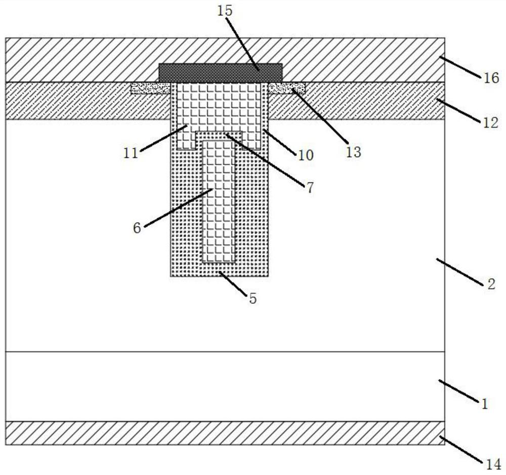
[0050] like Figures 3A to 3L As shown, it is a schematic diagram of the device structure of each step of the method according to the first embodiment of the present invention. Taking an N-type device as an example, the manufacturing method of a split-gate MOSFET according to the embodiment of the present invention includes the following steps:

[0051] Step one, as Figure 3A As shown, a lightly doped N-type epitaxial layer 2 is formed on a heavily doped N-type substrate 1, the upper surface of the N-type epitaxial layer 2 is the first main surface 001, and the N-type substrate The lower surface of 1 is the second main surface 002 .

[0052] Step two, as Figure 3B As shown, a first oxide layer 3 is deposited on the first main surface 001; the thickness of the first oxide layer 3 can be adjusted as required, and preferably, the first oxide layer 3 is silicon oxide.

[0053] Step three, as Figure 3C As shown, the first oxide layer 3 and the epitaxial layer 2 are etched to...

no. 2 example

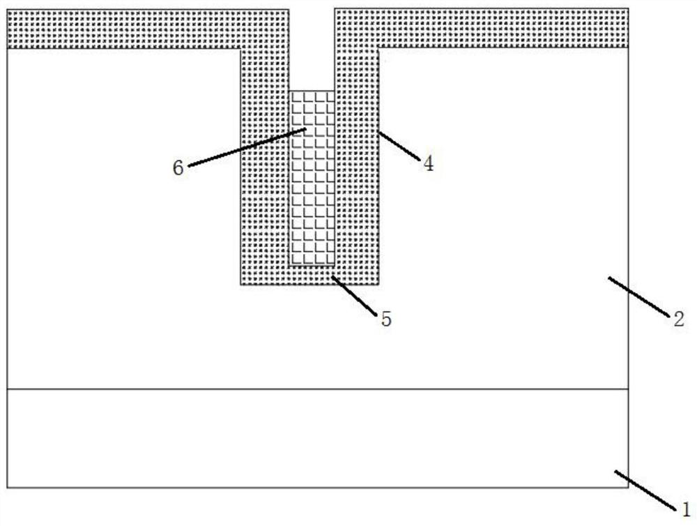
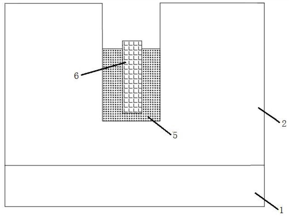
[0069] The difference between this embodiment and the first embodiment is that, as Figure 5 As shown, in this embodiment, the seventh step is to grow an oxide layer in the trench 4 by thermal oxidation, and form an inter-polysilicon isolation oxide layer 7 on the separation gate polysilicon 6 . Since the second oxide layer 5 is formed on the sidewall of the trench 4, oxygen cannot easily penetrate the second oxide layer 5 to react with the silicon in the N-type epitaxial layer 2 during thermal oxidation. Therefore, the polysilicon formed above the separation gate polysilicon 6 The thickness D1 of the isolation oxide layer 7 will be significantly greater than the increased thickness D3 of the second oxide layer 5 located on the sidewall of the trench 4 and the increased thickness D2 of the second oxide layer 5 located on the first main surface 001, and the thickness ratio can be It can reach 5:1 or more; in this step, an IPO that meets the process requirements can be formed at...


PUM


Abstract

The invention discloses a method for fabricating a split gate MOSFET, comprising: step 1, forming an epitaxial layer on a substrate; step 2, depositing a first oxide layer on a first main surface; step 3, forming a trench; Fourth, remove the first oxide layer; step five, form a second oxide layer in the trench; step six, form a separation gate polysilicon in the trench; step seven, form an isolation oxide layer between polysilicon; step eight, in the trench forming a nitride layer; step 9, forming sacrificial polysilicon in the trench; step 10, removing the nitride layer above the sacrificial polysilicon to form a mask structure; step 11, using the mask structure as an etching mask to remove the inter-polysilicon isolating the second oxide layer above the oxide layer; step 12, removing the nitride layer to lift off the sacrificial polysilicon. In the present invention, the isolation oxide layer between polysilicons that meets the technological requirements can be formed at one time through the high-density plasma chemical vapor deposition method or the low-temperature wet oxidation method.

Description

technical field [0001] The invention relates to the technical field of semiconductors, in particular to a manufacturing method of a split gate MOSFET. Background technique [0002] Trench power MOSFET is a new high-efficiency switching device developed after planar VDMOS. It is widely used in the field of power electronics due to its advantages of high input impedance, small driving current, fast switching speed, and good high temperature characteristics. High breakdown voltage, high current, and low on-resistance are the most critical indicators of power MOSFETs. The breakdown voltage is related to the on-resistance value. In the MOSFET design process, high breakdown voltage and low on-resistance cannot be obtained at the same time. balance between the two. [0003] In order to obtain a higher breakdown voltage and lower on-resistance as much as possible, a new type of MOSFET device with split gate structure has emerged. Compared with the common trench MOSFET structure, it...

Claims


Application Information

Patent Timeline
Patent Type & Authority Patents(China)
IPC IPC(8): H01L21/336H01L29/78H01L29/423
CPCH01L29/7813H01L29/66734H01L29/4236
Inventor 孙闫涛黄健张朝志顾昀浦宋跃桦吴平丽樊君张丽娜虞翔
Owner 捷捷微电(南通)科技有限公司
Why Eureka
Try Eureka