Method for preparing nickel silicide by laser annealing

A technology of nickel silicide and laser annealing, which is applied in the manufacture of electrical components, semiconductor/solid-state devices, circuits, etc., can solve the problems of slow annealing speed and affecting device performance, achieve fast heating annealing speed, avoid spikes, and reduce leakage The effect of current

Inactive Publication Date: 2014-03-26
SHANGHAI HUALI MICROELECTRONICS CORP
View PDF4 Cites 2 Cited by
  • Summary
  • Abstract
  • Description
  • Claims
  • Application Information

AI Technical Summary

Problems solved by technology

However, this patent also uses the traditional annealing process for annealing. Since the traditional annealing is to place the entire silicon wafer in a reaction furnace to heat all parts of the silicon wafer, it inevitably requires a large amount of energy for heating, and the annealing The speed is also slow. At the same time, because the nickel in the source and drain regions of the silicon wafer and the bottom of the gate stays at high temperature for a long time, it is easy to produce vertical diffusion or lateral diffusion, and it combines with deep Si to form a nickel silicide peak, which leads to leakage. current, which affects device performance

Method used


Image

  • Method for preparing nickel silicide by laser annealing
  • Method for preparing nickel silicide by laser annealing
  • Method for preparing nickel silicide by laser annealing

Examples


Embodiment Construction

[0026] The specific embodiment of the present invention will be further described below in conjunction with accompanying drawing:

[0027] The invention provides a method for forming nickel silicide by laser annealing, which is applied in a self-aligned nickel silicide process, comprising the following steps:

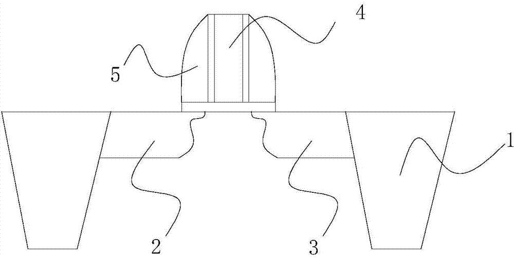
[0028] Step S1, providing a silicon wafer, including a silicon substrate, the silicon substrate is formed with a shallow trench isolation structure 1, and a source level 2 and a drain electrode 3 are formed between the shallow trench isolation structures, and the source level 2 and the drain electrode 3 A gate 4 is formed on the substrate between them, and a side wall 5 is formed on the side of the gate, such as figure 1 structure shown. The silicon wafer is cleaned to remove the oxide layer on its surface.

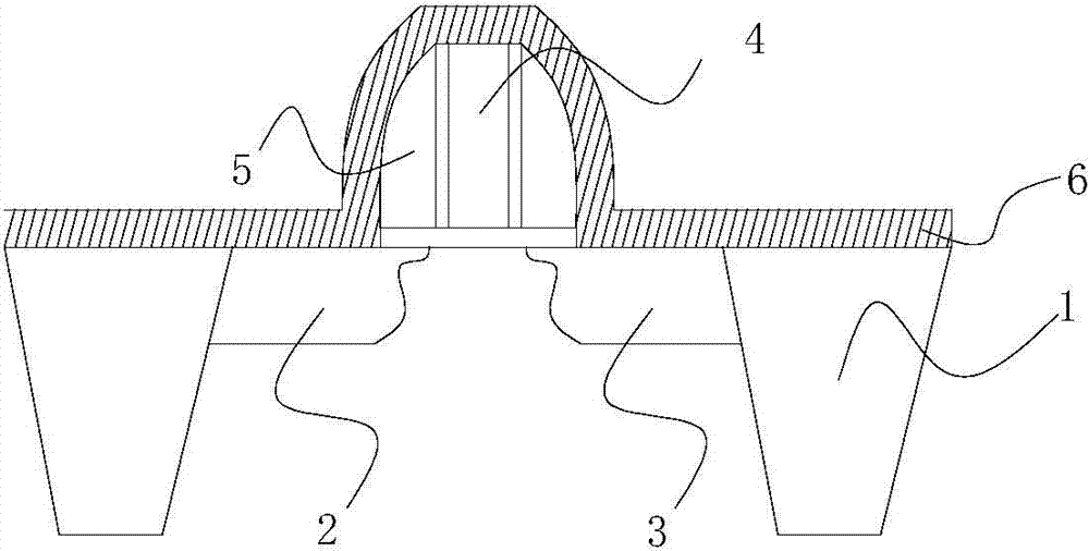
[0029] Step S2, depositing a cover layer 6 to cover the surface of the substrate and the top and sidewall surfaces of the gate. In an embodiment of the present...


PUM


Abstract

The invention discloses a method for preparing a nickel silicide by laser annealing. The nickel silicide is prepared by twice laser annealing processes, it is ensured that the temperatures of the twice laser annealing are kept within a certain range, and finally the nickel silicide with a relatively low resistivity can be obtained. Annealing is implemented through laser, so that compared with the traditional technology, the speed is higher, the working efficiency is greatly improved, and the production cost is reduced; and laser can be used to heat necessary positions of a silicon chip but not other positions, thereby avoiding that nickel is diffused at unnecessary positions and reacts with silicon to generate nickel silicide peaks which cause current leakage, and improving the performance of devices.

Description

technical field [0001] The invention relates to a process for forming nickel silicide in the semiconductor wafer production industry, in particular to a method for forming nickel silicide by laser annealing. Background technique [0002] As the integration of semiconductor devices continues to increase and the critical dimensions associated with these devices continue to decrease, how to manufacture semiconductor devices with low-resistance materials to maintain or reduce signal delay has become the focus of attention, while the gate conductors and The reduction of the sheet resistance and contact resistance of the source / drain region is equally important as the subsequent interconnection. Silicide and salicide materials and processes have been widely used to reduce the sheet resistance and contact resistance of gate conductors and source / drain regions of CMOS devices. [0003] Metals and alloys including titanium, cobalt and nickel have been used to form silicide layers on...

Claims


Application Information

Patent Timeline
Patent Type & Authority Applications(China)
IPC IPC(8): H01L21/324
CPCH01L21/823418H01L21/28H01L21/823437
Inventor 曹威傅昶
Owner SHANGHAI HUALI MICROELECTRONICS CORP
Why Eureka
Try Eureka