


Quick Research
Generate reliable direction feasibility study reports for your R&D in just a few steps.

Technical Q&A
Discover and master advanced knowledge NOW. Basics, ideas, possibilities, all at once.

Find Solutions
As an expert in R&D theories, this can generate solutions to your technical problems instantly.

Evaluate Feasibility
Analyze your overall solution with one click, know your potential R&D risks in advance.

Monitor Landscape
Get weekly tech updates, stay abreast of the latest tech innovations and key insights.
Electrostatic chuck
An electrostatic chuck and electrode layer technology, which is applied in the direction of holding devices, circuits, and electrical components that apply electrostatic attraction, can solve problems such as peeling, reduced internal electrode conductivity, and weak adhesion, so as to improve adhesion, The effect of improving the conductivity
- Summary
- Abstract
- Description
- Claims
- Application Information
AI Technical Summary
Problems solved by technology
Method used
Image

Examples
Embodiment 1
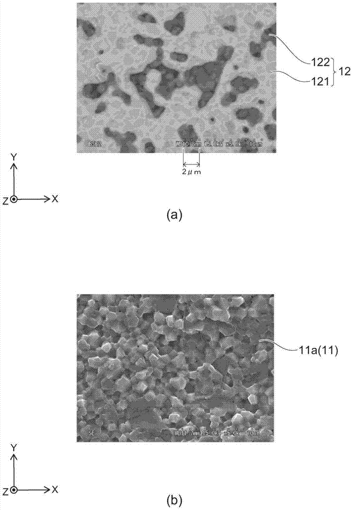
[0139] Example 1 is an example in which Pd is 50% by volume and alumina is 50% by volume. There is no problem with firing and grinding, and there is sufficient adhesion of the internal electrode layer. In addition, it has sufficient conductivity of the internal electrode layer when used in an electrostatic chuck.
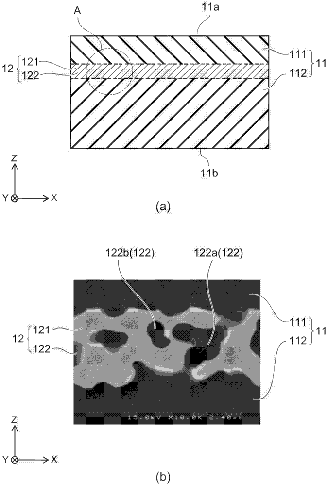
[0140] Figure 5 is a diagram illustrating an electrode layer.
[0141] Figure 5 A cross-sectional SEM image of the electrode layer 12 after firing is shown. Figure 5 The middle white part is Pd.
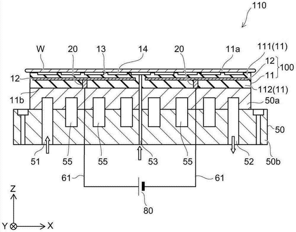
[0142] Such as Figure 5 As shown, the electrode layer 12 has no gaps and is dense, and the Pd particles are also closely attached to each other and continuous. Therefore, the electrical conductivity is also good, and the adhesion between the electrode layer 12 and the high-purity alumina layers (first dielectric layer 111 and second dielectric layer 112 ) above and below it is also in a good state.
[0143] In addition, since high-purity alumina and electrode ra...
Embodiment 2
[0144] Example 2 is an example in which Pd is 30% by volume and alumina is 70% by volume. Although the electrode layer 12 does not have conductivity after firing, sufficient conductivity for use in an electrostatic chuck can be secured by HIP treatment. In addition, there is no problem in firing and grinding, and sufficient adhesion force of the electrode layer 12 is exhibited.
[0145] Plasma Resistance Evaluation
[0146] Regarding the decrease in surface roughness (durability) of the alumina sintered body caused by plasma irradiation, a plasma irradiation test and evaluation were performed using the following samples. As test samples used, a part of the electrostatic chuck produced in Examples 1 and 2 was cut out, and the surface thereof was ground to a surface roughness of Ra of 0.03 μm or less. Plasma was irradiated to this test sample, and the change of surface roughness Ra was measured. Plasma irradiation was carried out at 1000W for 30 hours using a reactive ion etc...
PUM
| Property | Measurement | Unit |
|---|---|---|
| thickness | aaaaa | aaaaa |
| thickness | aaaaa | aaaaa |
| particle size | aaaaa | aaaaa |
Abstract
Description
Claims
Application Information
 - R&D Engineer
- R&D Manager
- IP Professional
- Industry Leading Data Capabilities
- Powerful AI technology
- Patent DNA Extraction
Browse by: Latest US Patents, China's latest patents, Technical Efficacy Thesaurus, Application Domain, Technology Topic, Popular Technical Reports.
© 2024 PatSnap. All rights reserved.Legal|Privacy policy|Modern Slavery Act Transparency Statement|Sitemap|About US| Contact US: help@patsnap.com