
Method for forming shallow trench isolation region

A shallow trench isolation area and trench technology, which is applied in electrical components, semiconductor/solid-state device manufacturing, circuits, etc., can solve the problem of incomplete etching of polysilicon gates, reduce adhesion, increase filling density, and improve performance Effect

Inactive Publication Date: 2014-03-26
SEMICON MFG INT (SHANGHAI) CORP
View PDF3 Cites 1 Cited by
  • Summary
  • Abstract
  • Description
  • Claims
  • Application Information

AI Technical Summary

Problems solved by technology

Subsequently, polysilicon gates are formed on the active regions on both sides of the shallow trench isolation region. It is likely that due to the existence of the recess, the etching of the polysilicon gates is incomplete, resulting in the electrical connection of the polysilicon gates on the two active regions.

Method used


Image

  • Method for forming shallow trench isolation region
  • Method for forming shallow trench isolation region
  • Method for forming shallow trench isolation region

Examples


Embodiment Construction

[0028] In order to make the object, technical solution and advantages of the present invention clearer, the present invention will be further described in detail below with reference to the accompanying drawings and examples.

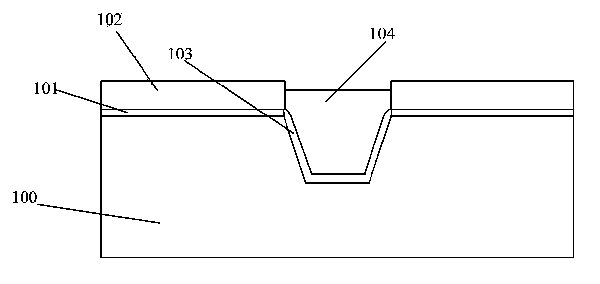
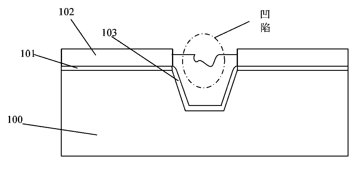
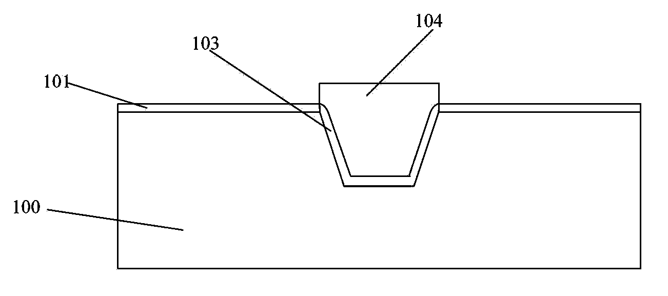
[0029] Please refer to the schematic diagram of the specific manufacturing process of the shallow trench isolation region of the present invention Figure 2a to Figure 2e , the flow chart of the specific production method is as follows figure 2 shown, including the following steps:

[0030] Step 21, sequentially forming an isolation oxide layer 101 and a silicon nitride layer 102 on the semiconductor substrate 100;

[0031] Specifically, an isolation oxide layer 101 is thermally oxidized and grown on the semiconductor substrate 100 to protect the active region from chemical contamination during the subsequent removal of the silicon nitride layer, and to serve as a barrier between the silicon nitride layer and the silicon substrate. Stress buffer laye...


PUM


Abstract

The invention discloses a method for forming a shallow trench isolation region. The method comprises the following steps: sequentially forming an isolation oxidation layer and a silicon nitride layer on a semiconductor substrate; sequentially etching the silicon nitride layer, the isolation oxidation layer and the semiconductor substrate, and forming a trench inside the semiconductor substrate; growing a liner silicon nitride layer on the surface inside the trench; filling and polishing an oxide inside the trench, forming the shallow trench isolation region, and eliminating the silicon nitride layer, wherein the step of filling the oxide inside the trench is performed by repeatedly using a method that the silicon nitride layer is formed through high-density plasma chemical vapor deposition with the combination of oxygen treatment. Through the adoption of the method, granular impurities can be effectively eliminated.

Description

technical field [0001] The invention relates to the manufacturing technology of semiconductor devices, in particular to a method for forming shallow trench isolation regions. Background technique [0002] The specific manufacturing method of the shallow trench isolation region in the prior art includes the following steps: [0003] Step 11, thermally oxidize and grow an isolation oxide layer 101 on the semiconductor substrate 100 to protect the active region from chemical contamination during the subsequent removal of the silicon nitride layer, and to serve as a barrier between the silicon nitride layer and the silicon substrate. a stress buffer layer, the semiconductor substrate is a silicon substrate; [0004] Step 12, depositing a silicon nitride layer 102 on the surface of the isolation oxide layer 101; wherein, the silicon nitride layer deposited in this step is a solid mask material; [0005] Step 13. Etching shallow trenches: sequentially etching the silicon nitride...

Claims


Application Information

Patent Timeline
IPC IPC(8): H01L21/762
CPCH01L21/76224H01L21/02271
Inventor 夏雁宾杨玲张飞
Owner SEMICON MFG INT (SHANGHAI) CORP
Learn More