Bipolar transistor with floating ring structure

A bipolar triode, floating ring technology, applied in semiconductor devices, electrical components, circuits, etc., can solve problems such as excessive electric field strength, and achieve the effects of slowing down aggregation, avoiding electric field strength, and high blocking voltage

Inactive Publication Date: 2014-03-26
SUZHOU YINGNENG ELECTRONICS TECH
View PDF8 Cites 1 Cited by
  • Summary
  • Abstract
  • Description
  • Claims
  • Application Information

AI Technical Summary

Problems solved by technology

[0004] The technical problem to be solved by the present invention is that in the prior art, the LBJT generates an excessively high electric field strength at the edge of the ohmic conta

Method used


Image

  • Bipolar transistor with floating ring structure

Examples


Embodiment 1

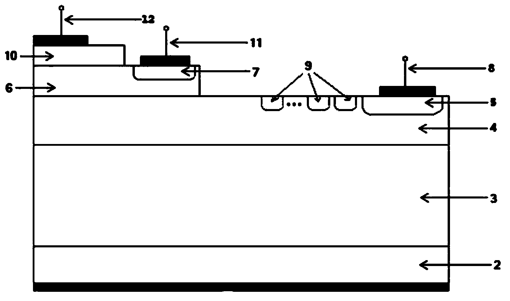
[0025] The structure of the bipolar triode with floating ring structure according to the present invention is as follows figure 1 As shown, the bipolar transistor here is an NPN lateral bipolar transistor (LBJT), which includes a substrate 2, a buffer zone 3, a collector region 4, a base region 6, and an emitter region 10 from bottom to top. Ohmic contact regions 7 and 5 are respectively formed at the boundaries of the base region 6 and the collector region 4, the emitter 12 is located on the emitter region 10, and the collector electrode 8 is located on the ohmic contact region 5 of the collector region 4 Above, the base 11 is located above the ohmic contact region 7 of the base region 6 . In this embodiment, the substrate 2 is P + Silicon carbide substrate, the buffer layer 3 on the upper layer is a silicon carbide epitaxial layer, and then the collector region 4 on the upper layer forms an ohmic contact region 5 in the collector region 4 by ion implantation, in the collect...

Embodiment 2

[0027] On the basis of Embodiment 1, the number of floating rings can be 1, 10, 40, 50, or 100, and generally 1-100 can be selected according to needs. In this embodiment, the number of the floating rings is 40, and the number here is set according to the material and size of the bipolar transistor. In order to ensure the gentle effect of the floating ring on the electric field of the ohmic contact area of ​​the collector area, the setting distance between the floating ring and the ohmic contact area of ​​the collector area is 0.5um, and the floating ring It is an annular floating region formed by ion implantation and annealing in the drift region of the collector region. The ions here can be selected from boron ions and aluminum ions. In this embodiment, boron ions are selected. In order to improve the breakdown resistance of the entire surface of the collector region, a plurality of floating rings may also be arranged on the surface of the collector region, and floating ring...


PUM


Abstract

The invention relates to a bipolar transistor with a floating ring structure. The bipolar transistor comprises a substrate, a buffer zone, a collector region, a base region and an emission area, wherein ohmic contact areas are respectively arranged on the boundaries of the collector region and the base region; an emitting electrode is positioned on the emission area; a collecting electrode is positioned on the ohmic contact area of the collector region; a base electrode is positioned on the ohmic contact area of the base region; a plurality of floating rings are arranged at the periphery of the ohmic contact area of the collector region, positioned on the surface of the collector region and close to the ohmic contact area. Due to the adoption of the scheme, the technical problem that over high electric field strength at the edge of the ohmic contact area of the collecting electrode caused by an LBJT suppresses the improvement of blocking voltage in the prior art is avoided. Therefore, the bipolar transistor can bear higher blocking voltage.

Description

technical field [0001] The invention relates to a bipolar transistor, in particular to a planar bipolar transistor with a floating ring, and belongs to the technical field of power electronics integration. Background technique [0002] With the development of electronic technology, the application of power electronic technology is more and more extensive. Due to the complexity of power electronic devices, there are certain obstacles in its popularization and promotion. Power electronics integration can integrate complex power electronic components, which greatly simplifies the complexity of electronic components. Therefore, the international power electronics community generally believes that power electronics integration technology is the most effective way to solve the obstacles faced by the development of power electronics technology. Hope for a way out. Among power electronic integrated components, planar power electronic devices have great application potential in the...

Claims


Application Information

Patent Timeline
IPC IPC(8): H01L29/739H01L29/45
CPCH01L29/7396H01L29/402H01L29/45
Inventor 崔京京张作钦
Owner SUZHOU YINGNENG ELECTRONICS TECH
Why Eureka
Try Eureka