Silicone lens for LED (Light Emitting Diode) packaging and manufacturing method thereof

A technology of LED packaging and silicone lens, which is applied in electrical components, circuits, semiconductor devices, etc., can solve problems such as broken gold wires, achieve the effects of saving mold costs, reducing the risk of broken gold wires, and improving light extraction efficiency

Inactive Publication Date: 2014-03-26
NANJING TECH CORP LTD
View PDF7 Cites 42 Cited by
  • Summary
  • Abstract
  • Description
  • Claims
  • Application Information

AI Technical Summary

Problems solved by technology

Because the stress generated by the lens during the high-temperature curing molding process will cause the gold wire in the package to break during long-term operation, the reliability of the product is greatly challenged

Method used


Image

  • Silicone lens for LED (Light Emitting Diode) packaging and manufacturing method thereof
  • Silicone lens for LED (Light Emitting Diode) packaging and manufacturing method thereof
  • Silicone lens for LED (Light Emitting Diode) packaging and manufacturing method thereof

Examples


Embodiment Construction

[0036] The embodiments of the present invention will be described in detail below with reference to the accompanying drawings, but the present invention can be implemented in many different ways defined and covered by the claims.

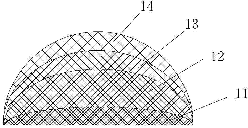
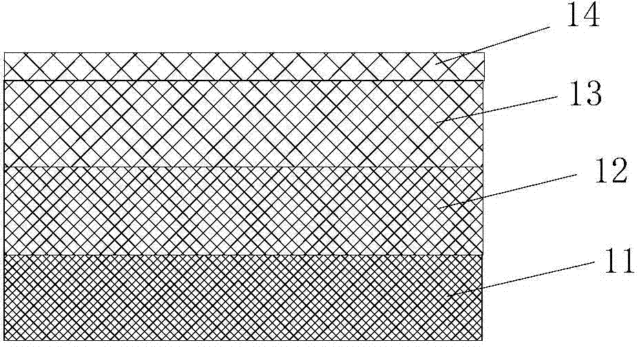
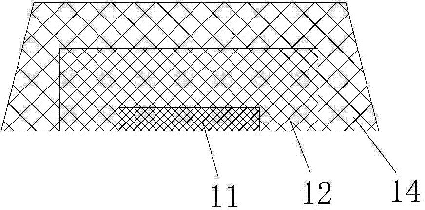
[0037] The invention relates to a multilayer silicone lens which can be used on LED devices. The shape of the lens is determined by the designer's requirements or the shape of the light source. It can be in the shape of a convex lens, flat or tubular. In particular, the silica gel lens is composed of at least two layers of silica gel with different refractive indices. The surface of the lens can be rough or finely structured, and some scattering particles can also be added. For multi-layer silicone lenses, the refractive index of the outermost layer is generally slightly lower than that of the inner layer. In addition, fluorescent materials such as fluorescent powder or quantum dots can be added to the outermost layer of the lens to adjust the colo...


PUM


Abstract

The invention discloses a silicone lens for LED (Light Emitting Diode) packaging, which is used for being adhered to the surface of a COB (Chip On Board) packaging body so as to improve the light extraction efficiency. The silicone lens is in a convex surface structure, and comprises at least two silicone layers arranged in sequence from inside to outside, wherein the refractive index of the silicone layer positioned on the outer layer is smaller than or equal to that of the silicone layer positioned on the inner layer. The multi-layer silicone lens disclosed by the invention can greatly improve the light extraction efficiency of an LED light source, particularly a high and medium power COB packaging body.

Description

technical field [0001] The invention relates to a silicone lens used for LED packaging and a manufacturing method thereof. Background technique [0002] At present, many manufacturers use epoxy resin to make lenses. However, the temperature stability of epoxy resin is poor, and it is easy to turn yellow under high temperature and high light intensity. It has high hardness and low elasticity, and it is easy to cause stress near the LED chip and gold wire, which will cause the gold wire to break and reduce the service life of the LED. [0003] In the process of LED packaging, silica gel is often used as a package to protect LED chips and gold wires from the damage of the external environment due to its good temperature resistance and low surface tension, and silica gel materials are used instead of epoxy resin to package LEDs. and lens trends, especially in high-power LED packages. [0004] The composition of silica gel is polydimethylsiloxane, which is an organic-inorganic ...

Claims


Application Information

Patent Timeline
Patent Type & Authority Applications(China)
IPC IPC(8): H01L33/00H01L33/58H01L33/48
CPCH01L33/54H01L33/58H01L2933/005H01L2933/0058
Inventor 付涛康永印陈文杰苏凯
Owner NANJING TECH CORP LTD
Why Eureka
Try Eureka