TFT, TFT array substrate, manufacturing method of TFT array substrate and display device

A technology of thin film transistors and array substrates, applied in the field of display devices, can solve problems such as breakdown of gate insulating layers, and achieve the effect of improving yield

Inactive Publication Date: 2014-04-09
BOE TECH GRP CO LTD
View PDF12 Cites 21 Cited by
  • Summary
  • Abstract
  • Description
  • Claims
  • Application Information

AI Technical Summary

Problems solved by technology

[0012] Embodiments of the present invention provide a thin film transistor, a TFT array substrate, a manufacturing method thereof, and a display devi

Method used


Image

  • TFT, TFT array substrate, manufacturing method of TFT array substrate and display device
  • TFT, TFT array substrate, manufacturing method of TFT array substrate and display device
  • TFT, TFT array substrate, manufacturing method of TFT array substrate and display device

Examples


Embodiment 1

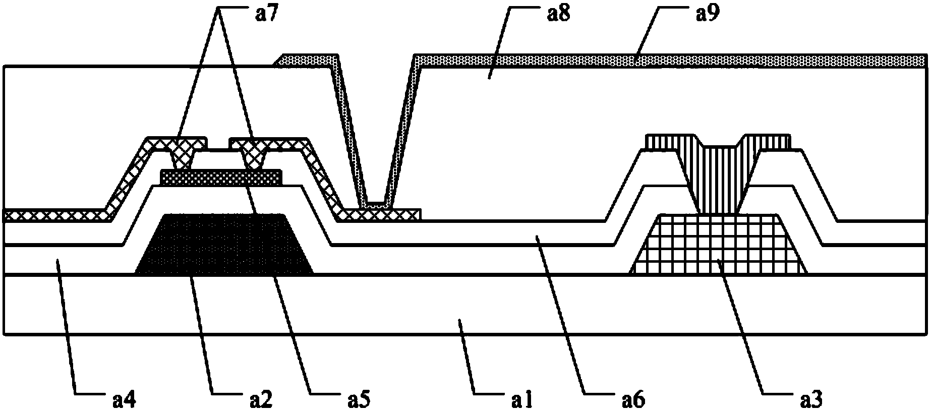
[0142] Embodiment 1. The manufacturing method of the TFT array substrate provided in this embodiment includes the following steps:

[0143] 1) Using a standard method to clean the transparent substrate substrate 1;

[0144] 2) Preparation of the gate electrode 2 and the lower electrode 3 of the storage capacitor, that is, using sputtering (sputter) or evaporation method to deposit a metal film with a thickness of 50 nm to 400 nm on the substrate, and perform patterning treatment to form a gate electrode 2 and the graph of the lower electrode 3 of the storage capacitor;

[0145] 3) Using plasma enhanced chemical vapor deposition (Plasma Enhanced Chemical Vapor Deposition, PECVD), deposit a SiOx film with a thickness of 100 nm to 500 nm on the substrate after the above steps to form the gate insulating layer 4;

[0146] 4) Deposit an IGZO thin film with a thickness of 10 nm to 80 nm on the base substrate that has completed the above steps by using the sputter method, and perfor...


PUM


Abstract

The embodiment of the invention provides a TFT, a TFT array substrate, a manufacturing method of the TFT array substrate and a display device. The TFT, the TFT array substrate, the manufacturing method of the TFT array substrate and the display device solve the problem that a grid insulation layer is prone to breakdown in terms of the structure of an existing bottom grid type TFT array substrate. A source electrode of the TFT comprises a first source electrode part, a drain electrode of the TFT comprises a first drain electrode part, the first source electrode part, the first drain electrode part and an active layer of the TFT are arranged on the same layer, and the first source electrode part and the first drain electrode part are located on the two sides of the active layer respectively and make direct contact with the active layer respectively. Because the first source electrode part and a grid electrode are not overlapped or very slightly overlapped and the first drain electrode part and the grid electrode are not overlapped or very slightly overlapped, capacitors will not be formed generally, and the phenomenon that the grid insulation layer is subjected to breakdown because the voltage of the source electrode or the voltage of the drain electrode is too large or the number of electrostatic charges gathering on the source/drain electrode is too large is avoided.

Description

technical field [0001] The present invention relates to the field of display manufacturing, in particular to a thin film transistor (Thin Film Transistor, TFT), a TFT array substrate including the thin film transistor, a manufacturing method thereof, and a display device including the TFT array substrate. Background technique [0002] Organic Light Emitting Diode (OLED) display has the advantages of self-illumination, wide viewing angle, high contrast ratio, thin profile, low power consumption, etc. It is one of the most concerned technologies in flat-panel display technology and has become the next-generation flat-panel display technology. The mainstream of display technology, more and more widely used. Generally, OLED displays have a stacked structure, using organic light-emitting compounds such as small molecule materials, polymers or other light-emitting materials as the organic light-emitting layer, which is placed between the cathode and the anode. According to differ...

Claims


Application Information

Patent Timeline
IPC IPC(8): H01L29/786H01L27/32H01L21/336
CPCH10K59/122H10K59/12H10K50/805H10K50/30H10K71/00H01L29/66969H01L29/78618H01L29/7869H01L27/1225H01L27/1288H10K59/00H10K59/1213H10K59/1216H01L29/66742H01L29/786
Inventor 王东方刘威陈海晶
Owner BOE TECH GRP CO LTD
Why Eureka
Try Eureka