Forming method of packaging structure

A technology of packaging structure and metal layer, which is applied in the manufacture of electrical components, electric solid-state devices, semiconductor/solid-state devices, etc. , the effect of increasing distance

Active Publication Date: 2014-04-16
NANTONG FUJITSU MICROELECTRONICS
View PDF5 Cites 11 Cited by
  • Summary
  • Abstract
  • Description
  • Claims
  • Application Information

AI Technical Summary

Problems solved by technology

[0004] The existing packaging structure occupies a large volume, which is not conducive to the improvement of the integration of the packaging structure

Method used


Image

  • Forming method of packaging structure
  • Forming method of packaging structure
  • Forming method of packaging structure

Examples


Embodiment Construction

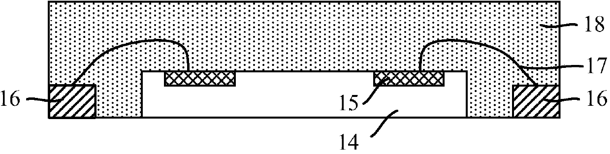
[0022] The integration level of the existing packaging structure is low, please refer to figure 1 , the pins 16 in the existing packaging structure are arranged around the semiconductor chip 14, and the pads 15 on the semiconductor chip 14 need to be electrically connected to the surrounding pins 16 through metal wires 17, so that the entire packaging structure occupies The larger volume is not conducive to the improvement of the integration degree of the packaging structure.

[0023] The invention provides a method for forming a packaging structure. The semiconductor chip is flipped over the pins, and the second metal bump on the semiconductor chip is welded together with the solder layer on the surface of the first metal bump, which reduces the size of the package. The volume of the structure increases the degree of integration.

[0024] In order to make the above objects, features and advantages of the present invention more comprehensible, specific embodiments of the pres...


PUM


Abstract

A forming method of a packaging structure comprises the steps that a lead frame metal layer is provided; the lead frame metal layer is etched, a plurality of independent pins are formed, and openings are formed between adjacent pins; firs metal protruding blocks are formed on the surfaces of the pins; welding-flux layers are formed on the surfaces of the top and the side wall of each first metal protruding block; a semiconductor chip is provided, a welding disc is formed on the surface of the semiconductor chip, and second metal protruding blocks are formed on the welding disc; the semiconductor chip is inversely arranged on the pins, and the second metal protruding blocks on the semiconductor chip and the welding-flux layers on the surfaces of the first metal protruding blocks are welded together. According to the method, the occupied area of the packaging structure is reduced, and the integration level of the packaging structure is improved.

Description

technical field [0001] The invention relates to the field of semiconductor packaging, in particular to a method for forming a semiconductor packaging structure. Background technique [0002] With the development of electronic products such as mobile phones and notebook computers towards miniaturization, portable, ultra-thin, multimedia and low-cost to meet the needs of the public, high-density, high-performance, high-reliability and low-cost packaging forms and their Assembly technology has developed rapidly. Compared with expensive packaging forms such as BGA (Ball Grid Array), new packaging technologies that have developed rapidly in recent years, such as Quad Flat No-lead Package (QFN) due to its good thermal performance and electrical The advantages of performance, small size, low cost and high productivity have triggered a new revolution in the field of microelectronic packaging technology. [0003] figure 1 It is a structural schematic diagram of an existing QFN pac...

Claims


Application Information

Patent Timeline
Patent Type & Authority Applications(China)
IPC IPC(8): H01L21/60
CPCH01L24/11H01L2224/16245H01L2224/11H01L2924/00012
Inventor 石明达石磊陶玉娟
Owner NANTONG FUJITSU MICROELECTRONICS
Why Eureka
Try Eureka