LED structure with high light extraction efficiency and manufacturing method thereof

A technology of LED structure and high light extraction, applied in electrical components, circuits, semiconductor devices, etc., can solve the problems of high technical difficulty, high cost, complex preparation process, etc., to improve the probability of vertical emission, improve light extraction efficiency, and low cost Effect

Inactive Publication Date: 2014-04-16
48TH RES INST OF CHINA ELECTRONICS TECH GROUP CORP
View PDF3 Cites 3 Cited by
  • Summary
  • Abstract
  • Description
  • Claims
  • Application Information

AI Technical Summary

Problems solved by technology

However, because the preparation process of this flip-chip photonic crystal structure is too complicated and tec

Method used


Image

  • LED structure with high light extraction efficiency and manufacturing method thereof
  • LED structure with high light extraction efficiency and manufacturing method thereof

Examples


Example Embodiment

[0039] The following describes the embodiments of the present invention through specific specific examples, and those skilled in the art can refer to the specific embodiments disclosed in this specification to understand other advantages and functions of the present invention. It should be understood that other embodiments may be utilized, and structural and functional modifications may be made without departing from the scope of the present invention.

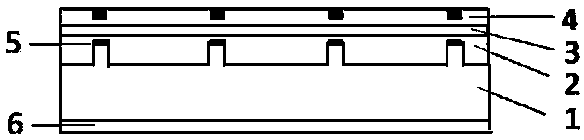
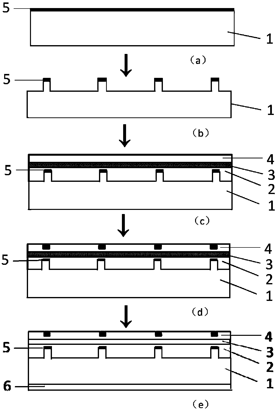
[0040] The LED structure with high light extraction efficiency provided by the present invention will be further described in detail below in conjunction with specific embodiments. figure 2 Shown is a method for preparing a GaN LED with a photonic crystal structure, including the following steps:

[0041] First proceed to step one, such as figure 2 (A) Shown. As a preferred solution of this embodiment:

[0042] The first step is to provide a sapphire pattern substrate 1, using SiH4 (silane) and NH3 (ammonia) as source gases, suc...


PUM

PropertyMeasurementUnit
Thicknessaaaaaaaaaa
Thicknessaaaaaaaaaa
Heightaaaaaaaaaa

Abstract

The invention discloses an LED structure with high light extraction efficiency and a manufacturing method of the LED structure. In order to improve the light extraction efficiency of the LED structure, the LED structure comprises a metal reflecting layer, a substrate, an LED epitaxial layer, a quantum well light-emitting layer and a P-type conducting layer, wherein the metal reflecting layer, the substrate, the LED epitaxial layer, the quantum well light-emitting layer and the P-type conducting layer are sequentially arranged from bottom to top, the upper surface of the substrate is provided with multiple columnar protrusions, a SiNx thin film layer is arranged between the upper surface of each columnar protrusion and the lower surface of the LED epitaxial layer, and the upper surface of the LED epitaxial layer is higher than the upper surface of each SiNx thin film layer. An LED which is provided with a photonic crystal structure and manufactured through the manufacturing method has the advantages of being low in manufacturing cost, simple, easy to obtain, high in efficiency and the like.

Description

technical field [0001] The invention relates to the technical field of light-emitting diode (LED) device manufacturing, and more particularly relates to an LED structure with high light extraction efficiency and a preparation method thereof. Background technique [0002] Semiconductor light-emitting diodes are widely used in white light lighting, backlight display, traffic signs, communication, signal indication, large-screen display and other fields due to their characteristics of energy saving, high efficiency, no pollution, small size, and long life, and meet the requirements of lightness, thinness, etc. miniaturization requirements. In particular, high-brightness light-emitting devices made of III-V semiconductor materials represented by GaN, AlGaN, InGaN, AlInGaN, etc., have attracted great attention due to their excellent luminous efficacy, and are considered to be the most ideal semiconductors in the future. One of the white light lighting sources. [0003] For GaN ...

Claims


Application Information

Patent Timeline
IPC IPC(8): H01L33/00H01L33/60H01L33/58H01L33/22
CPCH01L33/02H01L33/22H01L33/46
Inventor 韩云鑫魏唯陈峰武巩小亮
Owner 48TH RES INST OF CHINA ELECTRONICS TECH GROUP CORP
Why Eureka
Try Eureka