Array substrate, manufacturing method thereof and display device

An array substrate and substrate substrate technology, which is applied in semiconductor/solid-state device manufacturing, instruments, semiconductor devices, etc., can solve the problems of reducing the charging capacity of thin-film transistors, reducing the charging current of thin-film transistors, and large area of ​​thin-film transistors. area, improve charging capacity, and improve the effect of charging current

Inactive Publication Date: 2014-04-30
BEIJING BOE OPTOELECTRONCIS TECH CO LTD +1
View PDF6 Cites 20 Cited by
  • Summary
  • Abstract
  • Description
  • Claims
  • Application Information

AI Technical Summary

Problems solved by technology

[0005] 1) Due to the separation of the source and drain, the area of ​​the thin film transistor is larger, which reduces the aperture ratio of the pixel;
[0006] 2) Due to the separation of the source and the drain, the width-to-length ratio W / L of the thin film transistor channel is small, which reduces the charging current of the thin film transistor, thereby reducing the charging capacity of the thin film transistor

Method used


Image

  • Array substrate, manufacturing method thereof and display device
  • Array substrate, manufacturing method thereof and display device
  • Array substrate, manufacturing method thereof and display device

Examples


Embodiment Construction

[0036] In order to enable those skilled in the art to better understand the technical solutions of the present invention, the array substrate, the manufacturing method thereof, and the display device provided by the present invention will be described in detail below with reference to the accompanying drawings.

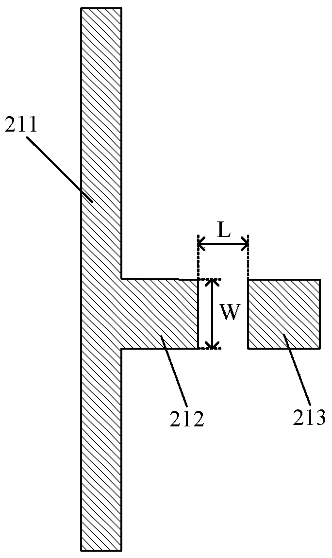
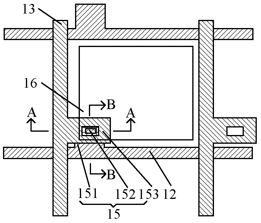
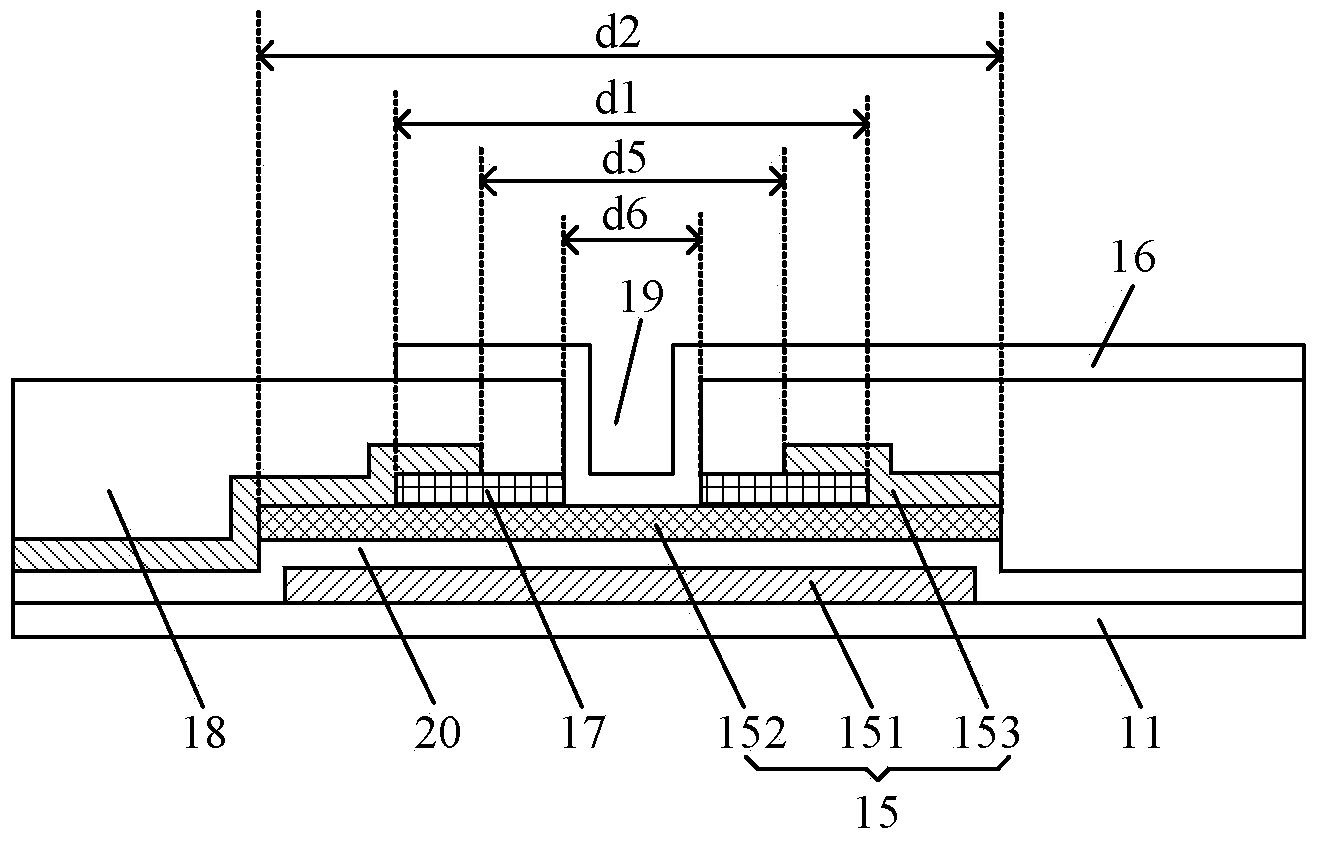
[0037] figure 2 Is a schematic diagram of the structure of an array substrate provided by the first embodiment of the present invention, image 3 for figure 2 A-A sectional view in the middle, Figure 4 for figure 2 B-B cross-sectional view, such as figure 2 , image 3 with Figure 4 As shown, the array substrate includes: a base substrate 11 and a gate line 12, a data line 13, a thin film transistor 15 and a pixel electrode 16 formed on the base substrate 11. The thin film transistor 15 includes a gate 151, an active layer 152 It is connected to the source-drain pattern 153, the source-drain pattern 153 is connected to the active layer 152, and the pixel electrode 16 ...


PUM


Abstract

The invention discloses an array substrate, a manufacturing method of the array substrate and a display device. The array substrate comprises a supporting base substrate, a grid line, a data line, pixel electrodes and a thin film transistor, wherein the grid line, the data line, the pixel electrodes and the thin film transistor are formed on the supporting base substrate. The thin film transistor comprises a grid electrode, an active layer and a source-drain electrode graph, the source-drain electrode graph is connected with the active layer, and the pixel electrodes are connected with the active layer. A source electrode and a drain electrode are arranged to be the source-drain electrode graph, the area of the thin film transistor is reduced, and therefore the aperture opening ratio of pixels is improved. The source electrode and the drain electrode are arranged to be one source-drain electrode graph, the width-to-length ratio W/L of a channel of the thin film transistor is increased, the charging current of the thin film transistor is improved, and therefore the charging capacity of the thin film transistor is improved.

Description

Technical field [0001] The present invention relates to the field of display technology, in particular to an array substrate, a manufacturing method thereof, and a display device. Background technique [0002] Liquid crystal displays are currently commonly used flat panel displays. Among them, Thin Film Transistor Liquid Crystal Display (TFT-LCD) is the mainstream product in liquid crystal displays. [0003] Among them, the array substrate is an important part of the thin film transistor liquid crystal display. In the prior art, an array substrate includes a base substrate and gate lines and data lines formed on the base substrate. The gate lines and data lines define a pixel unit. The pixel unit includes a thin film transistor and a pixel electrode. The thin film transistor includes: The gate electrode, the active layer, the source electrode and the drain electrode, and the pixel electrode is electrically connected to the drain electrode. At present, the channel of the thin film...

Claims


Application Information

Patent Timeline
Patent Type & Authority Applications(China)
IPC IPC(8): H01L27/12H01L29/786H01L29/417H01L21/77G02F1/1362G02F1/1368
CPCH01L29/41733H01L29/7869H01L27/124H01L27/1225H01L27/127H01L27/1222
Inventor 张家祥
Owner BEIJING BOE OPTOELECTRONCIS TECH CO LTD
Why Eureka
Try Eureka