InGaAs film grown on Si substrate and preparation method thereof

一种衬底、薄膜的技术,应用在生长在Si衬底上的InGaAs薄膜及其制备领域,能够解决很难精确控制成分、厚度、以及晶体质量、生长步骤繁琐、影响薄膜质量等问题,达到抑制界面的起伏、表面形貌好、简化外延生长工艺的效果

Active Publication Date: 2014-04-30
SOUTH CHINA UNIV OF TECH
View PDF3 Cites 20 Cited by
  • Summary
  • Abstract
  • Description
  • Claims
  • Application Information

AI Technical Summary

Problems solved by technology

But currently in 0.53 Ga 0.47 In the growth of As, most of them use buffer layer structures such as multi-layer composition gradient, composition jump, and composition inversion, which often result in the growth of In 0.53 Ga 0.47 It is necessary to epitaxially grow multiple thick buffer layers before the As material, the growth steps are cumbersome, and it is difficult to accurately control the composition, thickness, and crystal quality of each layer of material, which affects the final In 0.53 Ga 0.47 As film quality

Method used


Image

  • InGaAs film grown on Si substrate and preparation method thereof
  • InGaAs film grown on Si substrate and preparation method thereof
  • InGaAs film grown on Si substrate and preparation method thereof

Examples


Embodiment 1

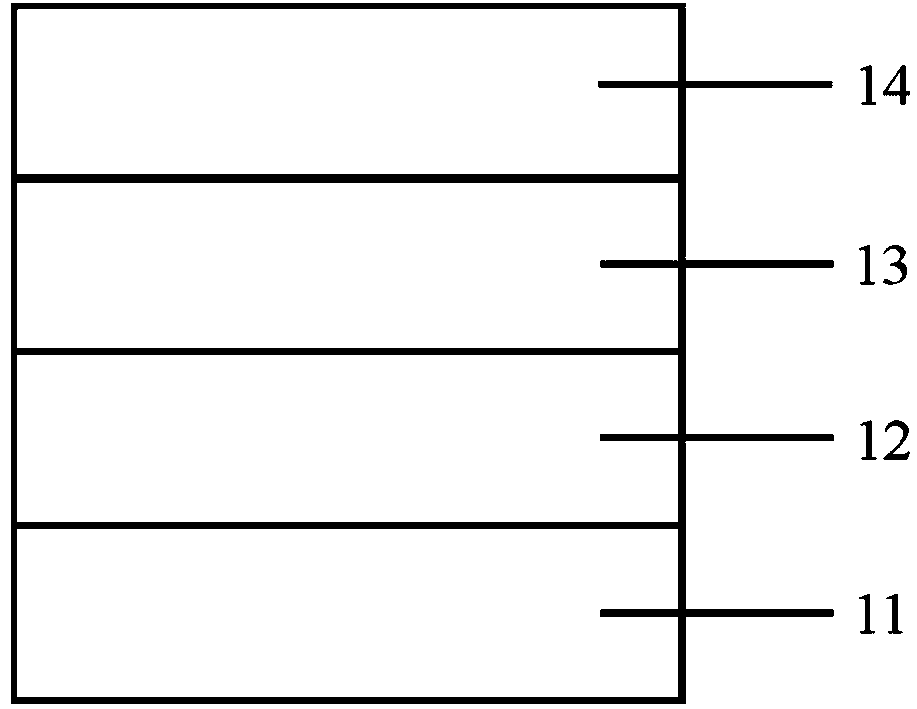
[0034] The preparation method of the InGaAs thin film grown on the Si substrate of the present embodiment comprises the following steps:

[0035] (1) Clean the Si substrate: wash with acetone and deionized water to remove organic matter on the surface of the substrate; place the Si substrate in HF:H 2 O=1:10 solution sonicated for 1 minute, concentrated H 2 SO 4 :H 2 o 2 :H 2 O=4:1:5 Ultrasound for 5 minutes, HF:H 2 Ultrasound in the O=1:10 solution for 1 minute, and finally rinsed with deionized water to remove surface oxides and organic matter; the cleaned Si substrate was dried with high-purity nitrogen;

[0036] (2) Pretreatment of the Si substrate: send the cleaned Si substrate into the molecular beam epitaxy sample chamber for pre-degassing for 15 minutes; then send it into the transfer chamber for degassing at 300°C for 0.5 hours; room;

[0037] (3) Deoxidize the Si substrate; after the Si substrate enters the growth chamber, raise the temperature of the Si subst...

Embodiment 2

[0044] The preparation method of the InGaAs thin film grown on the Si substrate of the present embodiment comprises the following steps:

[0045] (1) Clean the Si substrate: wash with acetone and deionized water to remove organic matter on the surface of the substrate; place the Si substrate in HF:H 2 O=1:10 solution sonicated for 3 minutes, concentrated H 2 SO 4 :H 2 o 2 :H 2 O=4:1:5 Ultrasound for 10 minutes, HF:H 2 Ultrasound in O=1:10 solution for 3 minutes, and finally rinsed with deionized water to remove surface oxides and organic matter; the cleaned Si substrate was dried with high-purity nitrogen;

[0046] (2) Pretreatment of the Si substrate: send the cleaned Si substrate into the molecular beam epitaxy sample chamber for pre-degassing for 30 minutes; room;

[0047] (3) Deoxidize the Si substrate; after the Si substrate enters the growth chamber, raise the temperature of the Si substrate to 1050°C and bake at high temperature for 15 minutes to remove the oxide...


PUM


Abstract

The invention discloses an InGaAs film grown on a Si substrate which comprises the Si substrate, a low-temperature In0.4Ga0.6As buffering layer, a high-temperature In0.4Ga0.6As buffering layer and an In0.53Ga0.47As expitaxial film. The low-temperature In0.4Ga0.6As buffering layer is grown at the temperature of 350 DEG C-380 DEG C. The high-temperature In0.4Ga0.6As buffering layer is grown at the temperature of 500 DEG C-540 DEG C. The sum of the thickness of the low-temperature In0.4Ga0.6As buffering layer and the thickness of the high-temperature In0.4Ga0.6As buffering layer is 10nm-20nm. The invention further discloses a preparation method of the InGaAs film. The InGaAs film grown on the Si substrate is good in crystalline quality, almost completely relaxes and is simple in preparation technology.

Description

technical field [0001] The invention relates to an InGaAs film and a preparation method thereof, in particular to an InGaAs film grown on a Si substrate and a preparation method thereof. Background technique [0002] III-V compounds are widely used in optoelectronic devices due to their advantages of good stability, small effective mass, high electron mobility and peak velocity, and high light absorption coefficient. Among them, In x Ga 1-x The forbidden band width of As (0≤x≤1) material can vary in the range of 0.35eV (InAs) to 1.43eV (GaAs) with the change of In composition. According to these characteristics, In x Ga 1-x As materials, especially In with an In composition of 0.53 0.53 Ga 0.47 As materials can be used in room temperature infrared detectors and high-efficiency tandem solar cells. [0003] Epitaxial growth In 0.53 Ga 0.47 Commonly used substrates for As materials are InP, GaAs and Si. However, InP and GaAs are expensive, the wafer size is small, and...

Claims


Application Information

Patent Timeline
Patent Type & Authority Applications(China)
IPC IPC(8): H01L31/0304H01L31/18
CPCH01L21/02381H01L21/02463H01L21/02502H01L21/02546H01L21/02631H01L31/03046H01L31/1844C30B25/183C30B29/42H01L21/02052H01L21/02433H01L21/0262H01L21/02658H01L29/201H01L31/1848H01L31/1852Y02E10/544
Inventor 李国强高芳亮管云芳温雷李景灵张曙光
Owner SOUTH CHINA UNIV OF TECH
Why Eureka
Try Eureka