Method for growing InGaAs film on GaAs substrate

A substrate and thin film technology, applied in the direction of single crystal growth, crystal growth, single crystal growth, etc., can solve the problem of difficult to precisely control composition, thickness, and crystal quality, low minority carrier lifetime of GaInNAs epitaxial materials, and limited quad-junction stacking. Solar cell current density and other issues, to achieve the effect of suppressing the fluctuation of the interface, simplifying the epitaxial growth process, and simplifying the buffer layer structure

Inactive Publication Date: 2012-07-11
SOUTH CHINA UNIV OF TECH
View PDF10 Cites 13 Cited by
  • Summary
  • Abstract
  • Description
  • Claims
  • Application Information

AI Technical Summary

Problems solved by technology

The ideal energy band matching of four-junction tandem solar cells is 1.8 / 1.4 / 1.0 / 0.67 eV. Through theoretical calculation, although 1eV GaInNAs material is suitable for the band gap and lattice size of the third-junction solar cell, the GaInNAs epitaxial material The low minority carrier lifetime severely limits the current density of four-junction tandem solar cells and becomes a key factor restricting the improvement of efficiency
[0005] At present, GaAs-based high-efficiency multi-junction tandem solar cells adopt buffer layer structures such as multi-layer composition gradient, composition jump, and composition inversion (such as figure 1 As shown), the buffer layers of these multilayer structures need epitaxial growth of multiple thicker buffer layers in the solar cell structure, the growth steps are cumbersome, and it is difficult to precisely control the composition, thickness, and crystal quality of each layer of material, so that Affects the final In 0.3 Ga 0.7 As film quality

Method used


Image

  • Method for growing InGaAs film on GaAs substrate
  • Method for growing InGaAs film on GaAs substrate
  • Method for growing InGaAs film on GaAs substrate

Examples


Embodiment Construction

[0036] The present invention will be described below in conjunction with the accompanying drawings and embodiments, but the present invention is not limited to the following examples.

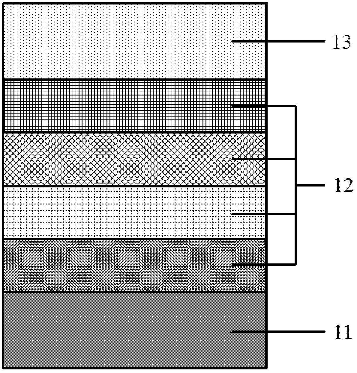
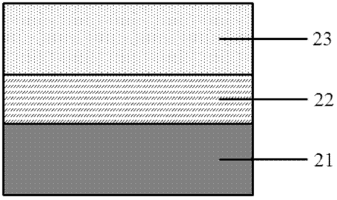
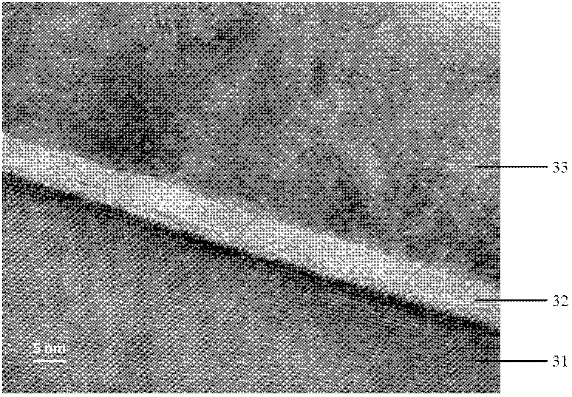
[0037] Such as figure 2 , image 3 shown. It is the method for growing an InGaAs thin film on a GaAs substrate of the present invention, comprising the following steps:

[0038] (1) GaAs substrate cleaning

[0039] The epitaxial substrate adopts (001) crystal orientation n-GaAs substrate. Ultrasonic removal of dirt particles on the surface of the GaAs substrate; washing with trichlorethylene, acetone, and methanol to remove surface organic matter; placing the GaAs substrate in 60°C H 2 SO 4 :H 2 o 2 :H 2 Etching in O (5:1:1) solution for 2 minutes; cleaning with HCl to remove surface oxides and organic matter; rinsing with deionized water; drying the cleaned GaAs substrate with filtered dry nitrogen;

[0040] (2) GaAs substrate pretreatment

[0041] After the GaAs substrate is cleane...


PUM


Abstract

The invention discloses a method for growing an InGaAs film on a GaAs substrate, which comprises the following steps of: (1) cleaning the GaAs substrate; (2) pre-processing the GaAs substrate; (3) deoxidizing; (4) growing a GaAs buffer layer; (5) growing a low-temperature single-layer In0.6Ga0.4As big-mismatch buffer layer; and (6) growing an In0.3Ga0.7As epitaxial film, wherein the In0.6Ga0.4As big-mismatch buffer layer and the In0.3Ga0.7As epitaxial film both can be prepared by using the molecular beam epitaxial growth or metal organic vapor deposition technology. Various defects caused by mismatch stress can be lowered by the big-mismatch buffer layer. The prepared In0.3Ga0.7As epitaxial layer has lower defect density. The method has the advantages of simple buffer layer structure, simple and convenient epitaxial growth process, low defect density of the In0.3Ga0.7As epitaxial film, high crystal quality and the like.

Description

technical field [0001] The invention is applied in the fields of solar cells, high electron mobility transistors, photodiodes, photodetectors and the like, and particularly relates to a method for growing an InGaAs thin film on a GaAs substrate. Background technique [0002] With the rapid development of the solar photovoltaic power generation industry and market, and driven by the demand for space vehicle energy systems, photovoltaic technology has continuously made important breakthroughs: crystalline silicon, amorphous silicon, polycrystalline silicon solar cells, III-V compound semiconductor cells, II -Group VI compound semiconductor cells, etc. More and more solar cell technologies are maturing. At the same time, the corresponding photoelectric conversion efficiency continues to increase, making today's photovoltaic technology more and more widely used in space and on the ground. The rapid development of GaAs-based III-V compound semiconductor cell technology is the mos...

Claims


Application Information

Patent Timeline
Patent Type & Authority Applications(China)
IPC IPC(8): C30B25/02C30B25/18C30B29/40
Inventor 李国强高芳亮
Owner SOUTH CHINA UNIV OF TECH
Why Eureka
Try Eureka