LED flip chip

A technology of flip-chip and lead electrodes, which is applied in the direction of electrical components, electrical solid devices, circuits, etc., can solve problems such as LED chip short circuit, cracked metal bumps, and affecting the reliability of LED chip work, so as to increase the welding area, The effect of reducing precision requirements

Inactive Publication Date: 2014-04-30
ELEC TECH PHOTOELECTRIC TECH DALIAN
View PDF5 Cites 7 Cited by
  • Summary
  • Abstract
  • Description
  • Claims
  • Application Information

AI Technical Summary

Problems solved by technology

[0008] see image 3 At the same time, in the flip-chip LED chip, the heat generated by the PN junction is mainly transferred to the heat-conducting substrate 82 or the outside world through the metal bumps 78, 79, because the thickness of the epitaxial structure of the flip-chip is only a few microns and it is compatible with the solder layer used for welding. 81 is close to each other. During the process of fixing the flip-chip LED chip and the heat-conducting substrate 82 and when the LED device is working under a relatively large current, the heat of welding or the heat generated by the operation of the LED chip will melt the solder layer 81, and the solder layer 81 After melting, it climbs from the metal bump of the semiconductor to the epitaxial structure, which causes a short circuit in the LED chip, resulting in the failure of the LED chip
[0009] like image 3 As shown, in the process of fixing the flip-chip LED chip and the heat-conducting substrate 82 and when the LED device is working under a relatively large current, the heat generated by welding or the heat generated by the operation of the LED chip will increase the temperature of the LED chip, and the heat-conducting substrate 82 generally Adopt FR4 circuit board, aluminum-based or copper-based PCB; due to the thermal stress generated by the difference in thermal expansion coefficient between the LED chip and the heat-conducting substrate 82, it may cause the LED chip to crack or the metal bumps to peel off due to thermal stress, affecting the work of the LED chip reliability

Method used


Image

  • LED flip chip
  • LED flip chip
  • LED flip chip

Examples


Embodiment Construction

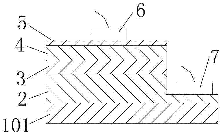
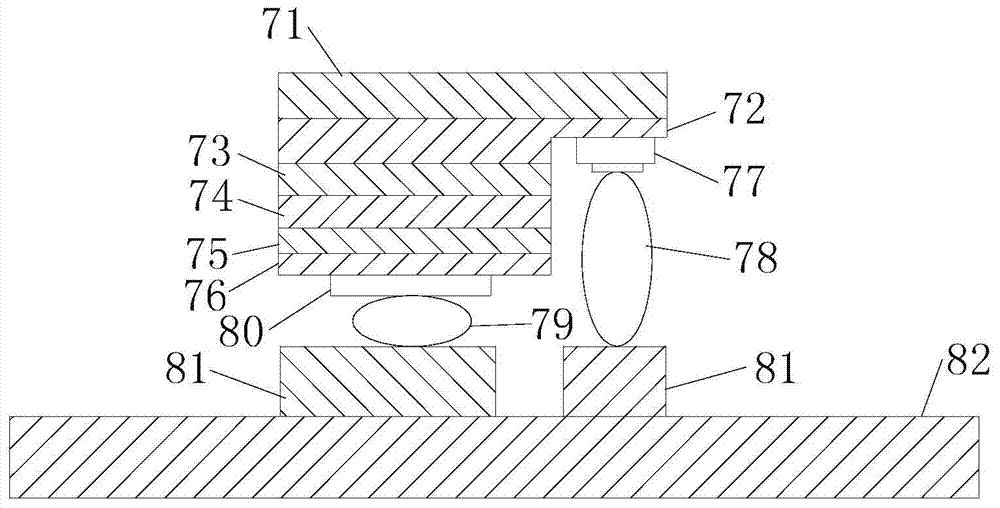
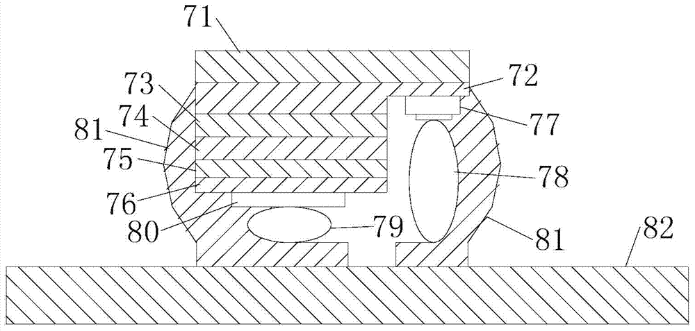
[0028] see Figure 4 and Figure 5 , LED flip-chip, including a sapphire substrate 1, sequentially arranged on the sapphire substrate 1 from bottom to top, and sequentially provided with an N-type layer 11, a light-emitting layer 12, a P-type layer 13, a reflective layer 15, The first insulating layer 16 . The first insulating layer 16 is provided with an N lead electrode 17 and a P lead electrode 18, and the N lead electrode 17 extends from the P-type layer 13 to the hole 14 of the N-type layer 11 along the depth (refer to Figure 9 ) is electrically connected to the N-type layer 11, and the P lead electrode 18 is electrically connected to the reflective layer 15. The N lead electrode 17 and the P lead electrode 18 are provided with a second insulating layer 22 , and the second insulating layer 22 is provided with a through hole 28 . The N pad layer 26 and the P pad layer 27 are respectively disposed on the second insulating layer 22 , and respectively contact the N lead e...


PUM


Abstract

The invention provides an LED flip chip. The LED flip chip comprises a sapphire substrate. An N type layer, a light emitting layer, a P type layer, a reflecting layer and a first insulating layer are sequentially arranged on the sapphire substrate from bottom to top. An N lead electrode and a P lead electrode are arranged on the first insulating layer, the N lead electrode extends from the P type layer to holes of the N type layer along the depth to be electrically connected with the N type layer, and the P lead electrode is electrically connected with the reflecting layer; the first insulating layer is further provided with an N bonding pad layer and a P bonding pad layer, wherein the N bonding pad layer is electrically connected with the N lead electrode, and the P bonding pad layer is electrically connected with the P lead electrode; second insulating layers are arranged on the N lead electrode and the P lead electrode, through holes are formed in the second insulating layers, the N bonding pad layer and the P bonding pad layer make contact with the N lead electrode and the P lead electrode respectively through the through holes, the first insulating layer or/and the second insulating layers are materials which do not absorb visible spectrums and have certain elasticity, and Young modulus of the materials ranges from 0.1GPa to 5GPa.

Description

technical field [0001] The invention relates to the technical field of LEDs, in particular to an LED flip chip. Background technique [0002] The structure of traditional positive-mounted GaN-based LED chips on sapphire substrates, such as figure 1 As shown, an N-type GaN layer 2, a quantum well QW active region 3, a P-type GaN layer 4, and a current spreading layer 5 are sequentially arranged on the substrate 101 from bottom to top, and on the current spreading layer 5 and the N-type GaN layer P electrodes 6 and N electrodes 7 are arranged in distribution. In this structure, the P electrode 6 is just located on the light-emitting surface of the chip; at the same time, a small part of the P-type GaN layer 4 and the quantum well QW active region 3 are etched, so that the N-electrode 7 forms an electrical connection with the N-type GaN layer 2 below. touch. Light is taken out from the upper P-type GaN layer 4 , and the limited electrical conductivity of the P-type GaN layer...

Claims


Application Information

Patent Timeline
Patent Type & Authority Applications(China)
IPC IPC(8): H01L33/00H01L33/48H01L33/64
CPCH01L33/56H01L2933/005H01L2224/14H01L2224/49107
Inventor 王冬雷莫庆伟
Owner ELEC TECH PHOTOELECTRIC TECH DALIAN
Why Eureka
Try Eureka