Method for forming patterned metal hard mask in interconnected structure

A technology for patterning metal and metal hard mask layers, which is applied in the fields of electrical components, semiconductor/solid-state device manufacturing, circuits, etc., and can solve the problems of reduced reliability of semiconductor devices and differences in the thickness of metal hard masks

Active Publication Date: 2014-05-07
SEMICON MFG INT (SHANGHAI) CORP
View PDF3 Cites 7 Cited by
  • Summary
  • Abstract
  • Description
  • Claims
  • Application Information

AI Technical Summary

Problems solved by technology

[0005] In view of this, the present invention provides a method for forming a patterned metal hard mask in an interconnection structure to solve the problem of the metal hard mask formed by physical vapor deposition in the prior art in the wafer edge region and the wafer middle region. There is a difference in thickness, which causes a problem that the reliability of semiconductor devices decreases

Method used


Image

  • Method for forming patterned metal hard mask in interconnected structure
  • Method for forming patterned metal hard mask in interconnected structure
  • Method for forming patterned metal hard mask in interconnected structure

Examples


Embodiment Construction

[0018] In order to make the purpose, technical solution and advantages of the present invention more clear, the present invention will be further described in detail below with reference to the accompanying drawings and examples.

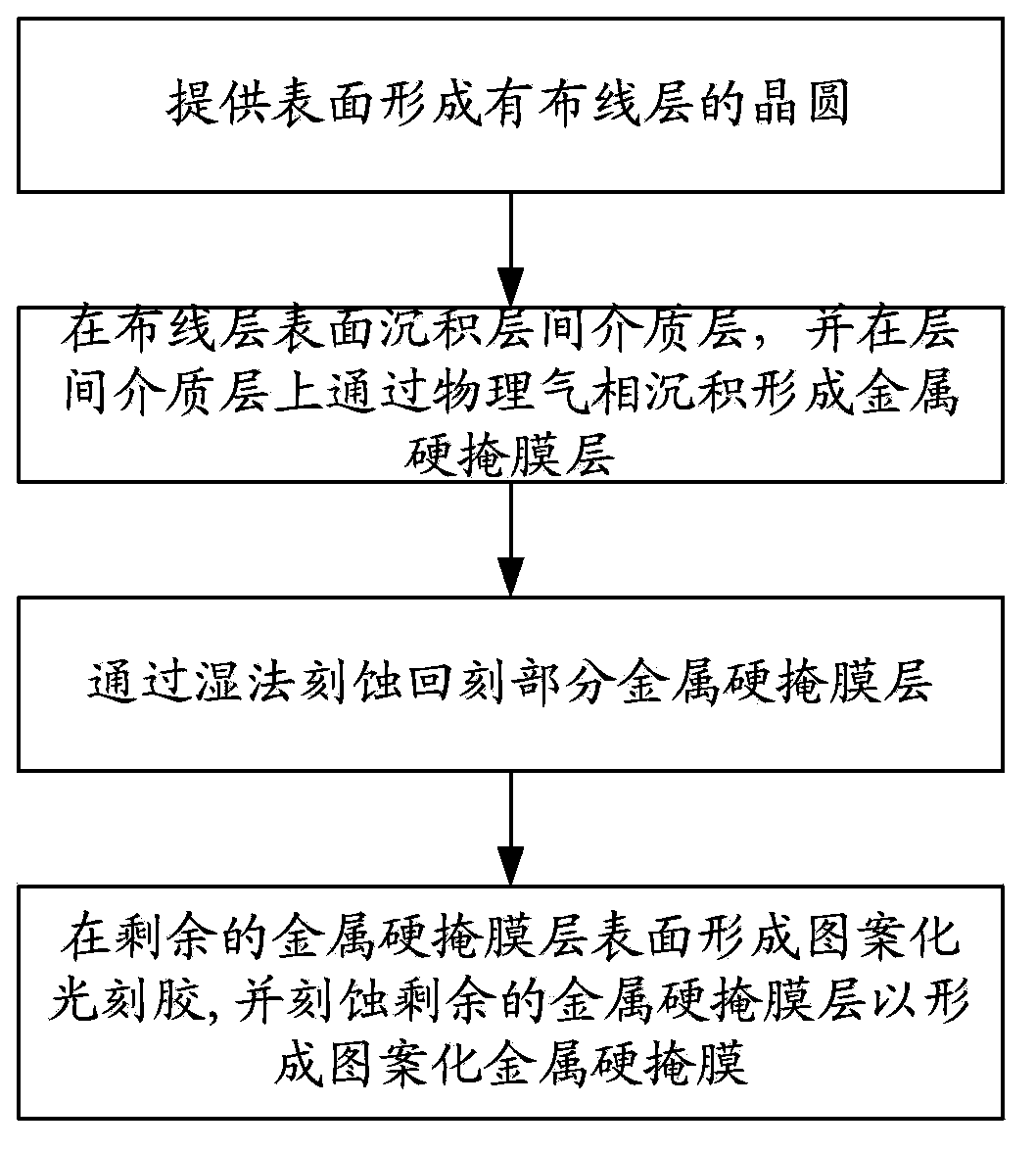
[0019] Such as figure 2 As shown, the present invention provides a method for forming a patterned metal hard mask in an interconnect structure, comprising:

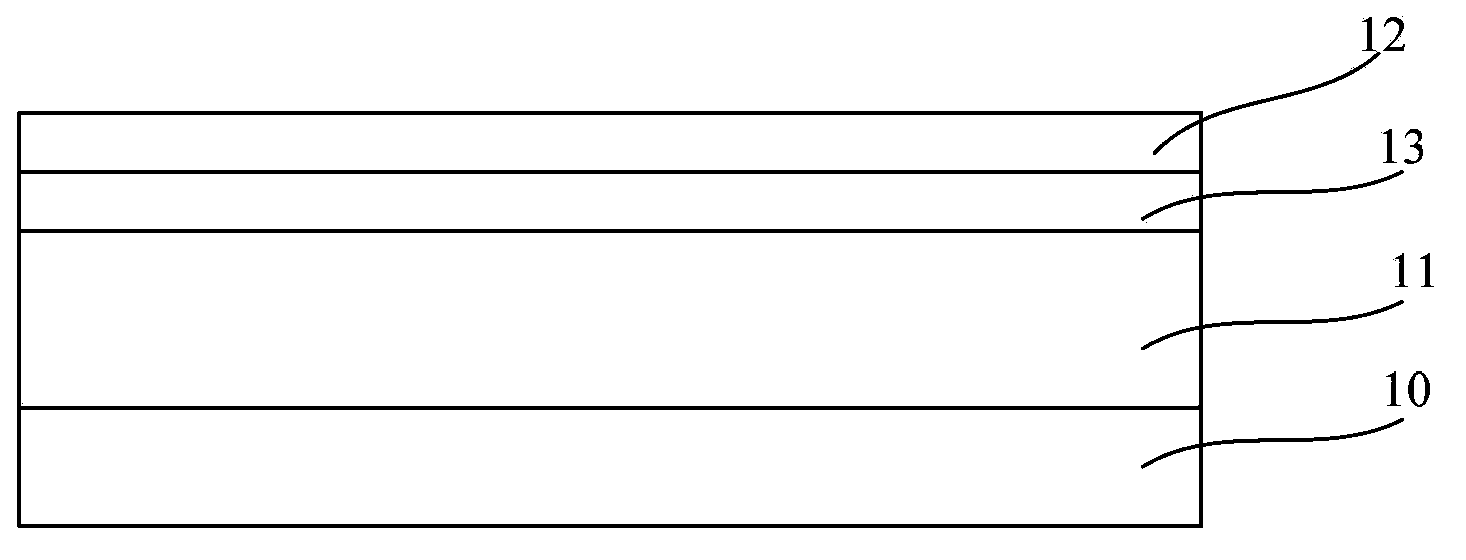
[0020] providing a wafer with a wiring layer formed on its surface;

[0021] An interlayer dielectric layer is deposited on the surface of the wiring layer, and a metal hard mask layer is formed on the interlayer dielectric layer by physical vapor deposition;

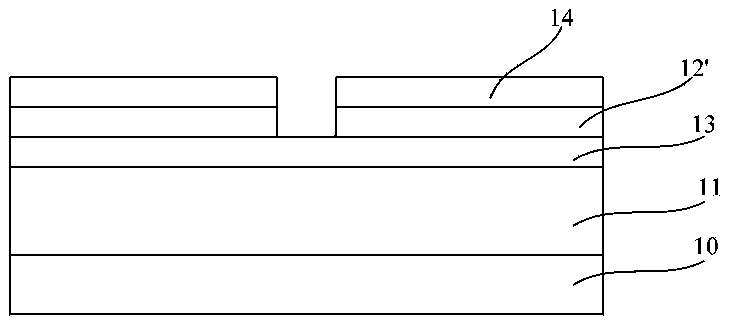
[0022] Etching back part of the metal hard mask layer by wet etching;

[0023] forming a patterned photoresist on the surface of the remaining metal hard mask layer;

[0024] The remaining metal hard mask layer is etched using the patterned photoresist as a mask to form a patterned metal hard mask.

[0025] As a typical embodiment o...


PUM


Abstract

The invention provides a method for forming patterned metal hard mask in an interconnected structure. By means of a property that etching rate on the middle position of an etched object is more than that on the edge position of the etched object in wet etching, primary etching back is executed on the metal hard mask formed by physical vapor deposition in order that a metal hard mask layer with uniform thickness is obtained. Further, the patterned metal hard mask is provided with uniform thickness on the middle position and the edge position of a wafer. Thus, a problem in the prior art is prevented that hollows occur to conductive material filled subsequently and influence the performance of a semiconductor device, wherein the hollows arise from a fact that good etching morphology cannot be acquired when connecting holes are subsequently etched by a dry etching method because difference exists in the thickness of the metal hard mask on a same wafer.

Description

technical field [0001] The invention relates to the field of semiconductor manufacturing, in particular to a method for forming a patterned metal hard mask in an interconnection structure. Background technique [0002] With the rapid development of semiconductor device manufacturing technology, semiconductor devices already have deep submicron structures, and integrated circuits contain a large number of semiconductor components. In such large-scale integrated circuits, high-performance, high-density connections between components are not only interconnected in a single interconnect layer, but also interconnected between multiple layers. Therefore, a multilayer interconnection structure is generally provided in which a plurality of interconnection layers are stacked on each other with an interlayer dielectric layer interposed therebetween for connecting semiconductor elements. A conventional method generally uses a Damascene dual damascene process to form a connection hole ...

Claims


Application Information

Patent Timeline
Patent Type & Authority Applications(China)
IPC IPC(8): H01L21/768
CPCH01L21/0337H01L21/31144H01L21/76802
Inventor 刘焕新
Owner SEMICON MFG INT (SHANGHAI) CORP
Why Eureka
Try Eureka