Preparing method for indium gallium zinc oxide semi-conductor film
A technology of indium gallium zinc oxide and semiconductor, which is applied in the field of preparation of indium gallium zinc oxide semiconductor thin film and preparation of indium gallium zinc oxide transistor, which can solve the problems of voids, many IGZO films, IGZOTFT performance attenuation, etc., and achieve simple preparation process , Improve device performance, the effect of excellent device performance
- Summary
- Abstract
- Description
- Claims
- Application Information
AI Technical Summary
Problems solved by technology
Method used
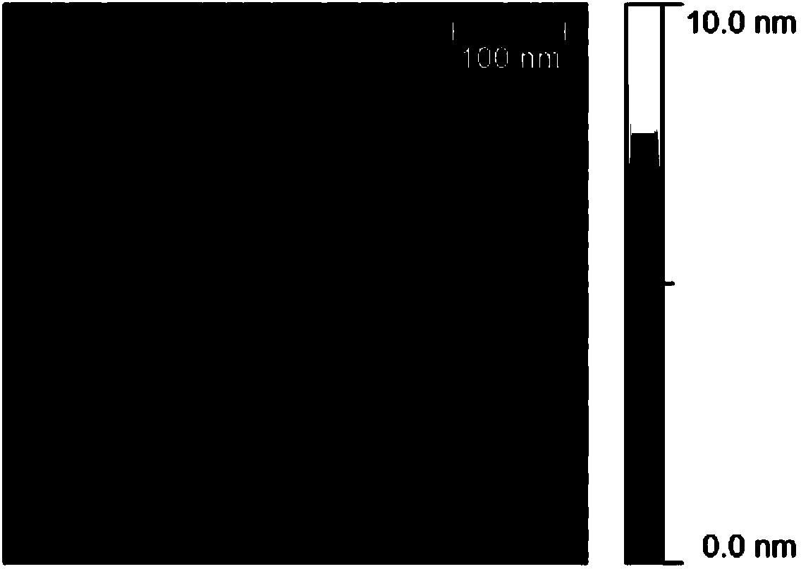
Image

Examples
Embodiment Construction
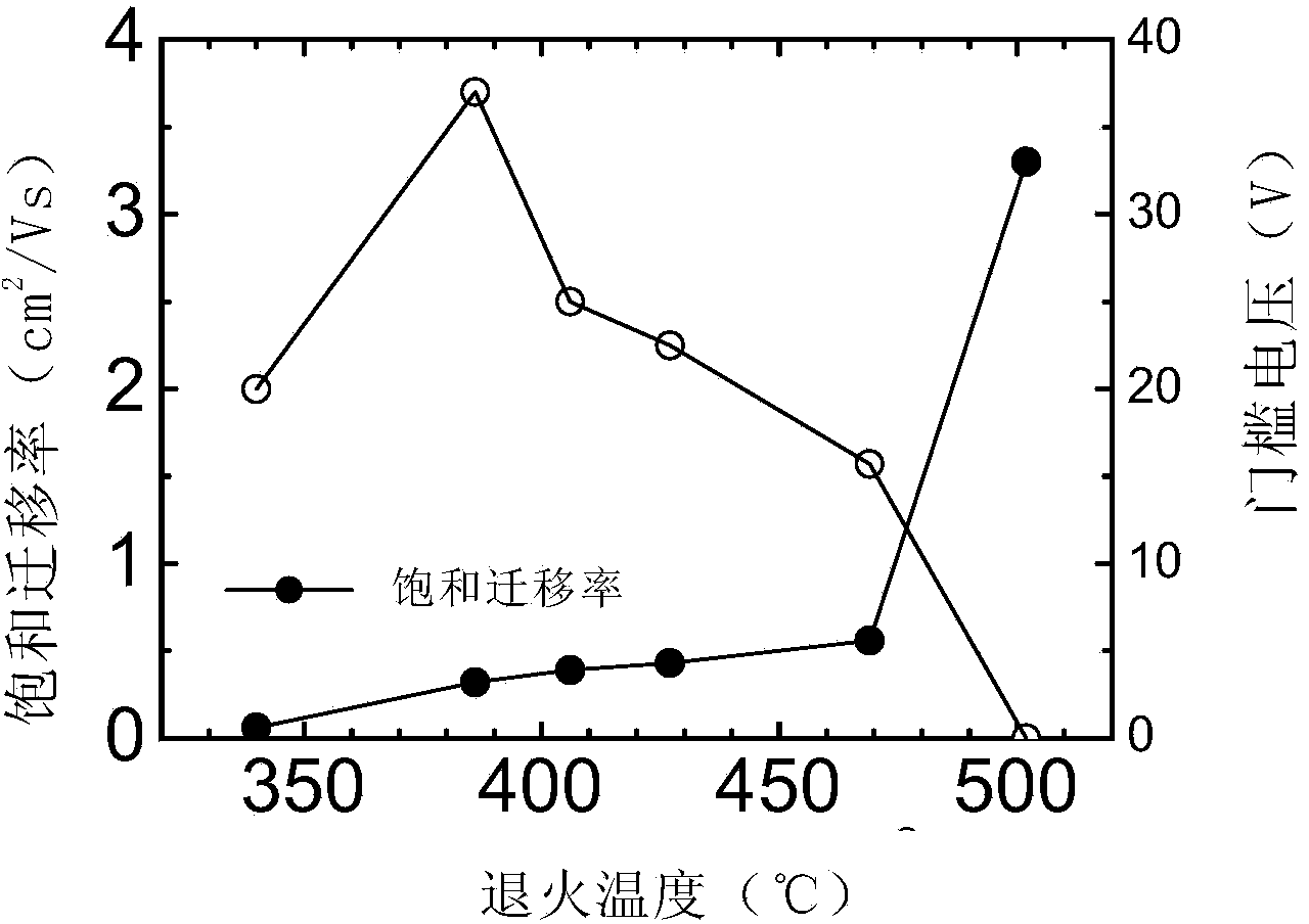
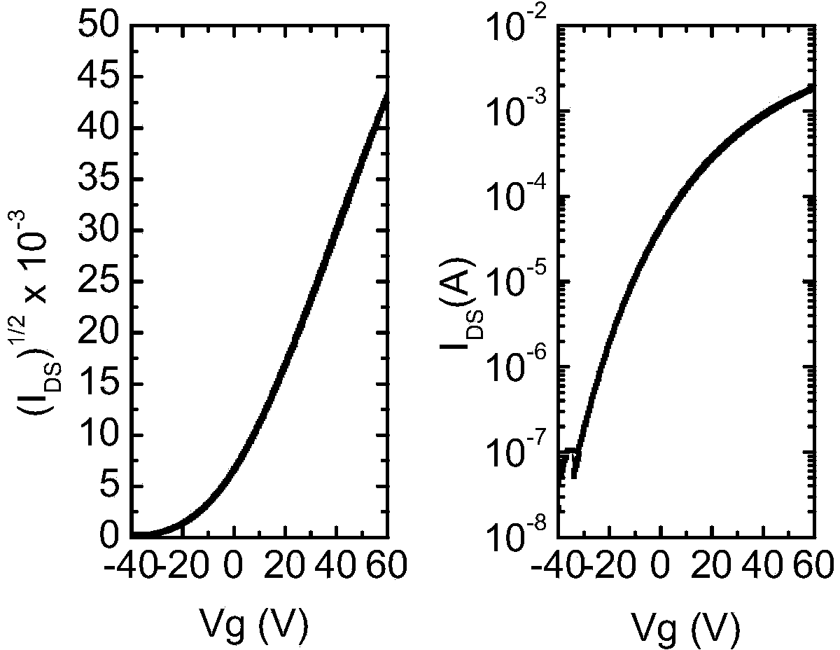
[0039] In one embodiment of the present invention, a method for preparing an indium gallium zinc oxide semiconductor thin film by a solution method comprises the following steps:
[0040] The first step, weigh 0.05 mg of gallium acetylacetonate [Ga(C 5 h 7 o 2 ) 3 ] powder and 0.05 mg [Zn(C 5 h 7 o 2 ) 2 ·xH 2 O] powder is dissolved in ethanol solvent, obtain gallium acetylacetonate solution and zinc acetylacetonate solution; Weigh 0.05 mg of indium acetylacetonate [In(C 5 h 7 o 2 ) 3 ] The powder was dissolved in tetrahydrofuran to obtain a solution of indium acetylacetonate.
[0041] The second step is to mix gallium acetylacetonate solution, zinc acetylacetonate solution and indium acetylacetonate solution with different volume ratios according to the molar ratio of gallium, zinc and indium in the precursor solution as x:y:z.
[0042] Correspondingly, gallium, zinc and indium in the precursor solution are x moles, y moles, z moles respectively, C 5 h 7 o 2 Th...
PUM
 Abstract
Description
Claims
Application Information
 - R&D
- Intellectual Property
- Life Sciences
- Materials
- Tech Scout
- Unparalleled Data Quality
- Higher Quality Content
- 60% Fewer Hallucinations
Browse by: Latest US Patents, China's latest patents, Technical Efficacy Thesaurus, Application Domain, Technology Topic, Popular Technical Reports.
© 2025 PatSnap. All rights reserved.Legal|Privacy policy|Modern Slavery Act Transparency Statement|Sitemap|About US| Contact US: help@patsnap.com