Eureka AIR delivers breakthrough ideas for toughest innovation challenges, trusted by R&D personnel around the world.

MTP memory cell

A technology of memory cells and capacitors, which is used in information storage, static memory, read-only memory, etc., and can solve problems such as punchthrough and punch-through.

Inactive Publication Date: 2014-05-14
SHANGHAI HUAHONG GRACE SEMICON MFG CORP
View PDF5 Cites 0 Cited by
  • Summary
  • Abstract
  • Description
  • Claims
  • Application Information

AI Technical Summary

Problems solved by technology

The reason is that under high voltage, if the N well spacing is not sufficient, it is easy to cause punch through (punch through), and the N well spacing directly affects the area of ​​the MTP memory cell

Method used


Image

  • MTP memory cell
  • MTP memory cell
  • MTP memory cell

Examples


Embodiment Construction

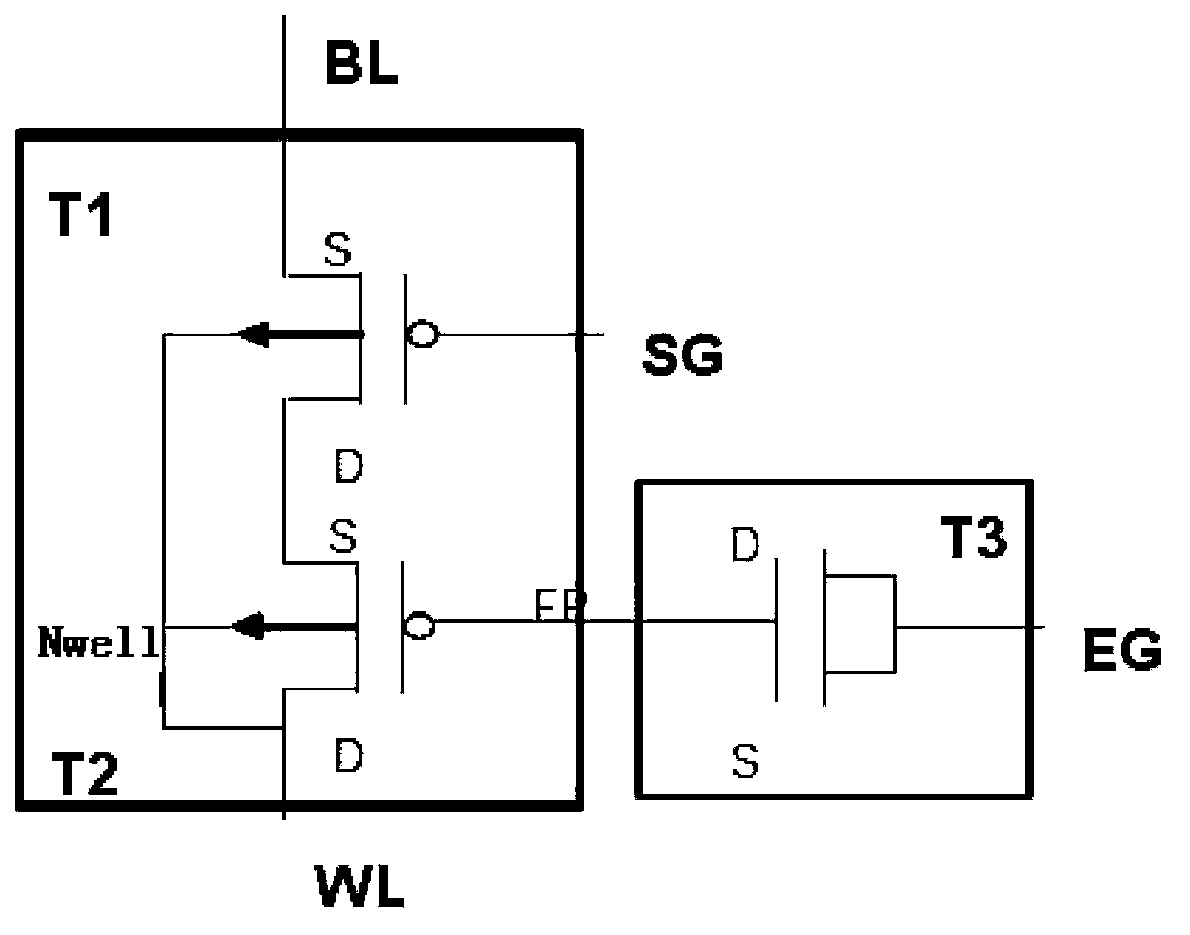
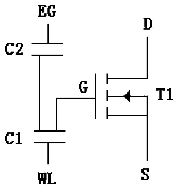
[0051] Such as image 3 As shown, the MTP storage unit of the present invention includes: the selection transistor N1 is an NMOS transistor, the programming capacitor C1 is an NWC capacitor, and the erasing capacitor C2 is a MIP capacitor;

[0052] Selecting the drain terminal D of the transistor N1 as the bit line BL of the MTP storage unit, and selecting the source terminal S of the transistor N1 as the source terminal SG of the entire MTP storage unit;

[0053] The upper plate of the programming capacitor C1 is connected to the gate G of the selection transistor N1, which is the same floating gate;

[0054] The lower plate of the programming capacitor C1 is the word line WL of the entire MTP memory cell.

[0055] The upper plate of the erasing capacitor C2 is used as the erasing terminal EG of the MTP;

[0056] The lower plate of the erasing capacitor C2 is connected to the upper plate of the programming capacitor C1, which are the same floating gate.

[0057] Wherein, the...


PUM


Abstract

The invention discloses an MTP memory cell. The MTP memory cell comprises a select transistor N1, a programmable capacitor C1 and an erasable capacitor C2. The drain gate of the select transistor N1 is adopted as the bit line BL of the MTP memory cell. The source gate of the select transistor N1 is adopted as the source gate SG of the whole MTP memory cell. The upper polar plate of the programmable capacitor C1 and the grid electrode of the select transistor N1 are connected and share a common floating poly. The lower polar plate of the programmable capacitor C1 is adopted as the word line WL of the whole MTP memory cell. The upper polar plate of the erasable capacitor C2 is adopted as the erase gate EG of the MTP. The lower polar plate of the erasable capacitor C2 and the upper polar plate of the erasable capacitor C1 are connected and share a common floating gate. According to the MTP memory cell provided by the invention, improvement and optimization are made to a traditional MTP memory cell, common logic processes can be embed and extra masks and technology are not needed. The MTP memory cell provided by the invention has a wider application scope and has high programming efficiency on various digital and digital-analog hybrid technology platforms. Compared with an MTP memory cell at present, the MTP memory cell provided by the invention has higher programming efficiency and better erase performances and reliability, and can decrease the area of the MTP memory cell.

Description

technical field [0001] The invention relates to the field of semiconductor manufacturing, in particular to an MTP storage unit. Background technique [0002] Using Floating poly (floating gate) to store electrons is a common MTP (Multi-time programmable) device (such as figure 1 , figure 2 As shown), it can be embedded in a common logic process without adding additional masks and processes, such as US Patent US7515478B2. The MTP of this structure is composed of three PMOS devices, using PMOS hot electron injection (CHE) for programming, and FN tunneling mechanism for data erasure of memory cells. The MTP memory cell with this structure is the most commonly used device architecture in the semiconductor industry at present. [0003] The programming process is accomplished through the hot electron effect (CHE). When the gate oxide film of the programming transistor T2 is thicker, the energy required for the channel current to decrease and the hot electrons to penetrate the ...

Claims


Application Information

Patent Timeline
Patent Type & Authority Applications(China)
IPC IPC(8): G11C16/02
Inventor 仲志华
Owner SHANGHAI HUAHONG GRACE SEMICON MFG CORP
Why Eureka
Eureka Blog
Learn More