Eureka AIR delivers breakthrough ideas for toughest innovation challenges, trusted by R&D personnel around the world.

Floating gate type flash synapse device structure and preparation method thereof

A technology of synapse device and floating gate type, which is applied in the field of floating gate type FLASH synapse device structure and its preparation, can solve the problems of low integration and complex structure, and achieve structural and process compatibility, simple steps, and wide application prospects Effect

Active Publication Date: 2022-08-02
58TH RES INST OF CETC
View PDF4 Cites 0 Cited by
  • Summary
  • Abstract
  • Description
  • Claims
  • Application Information

AI Technical Summary

Problems solved by technology

[0004] The purpose of the present invention is to provide a floating gate type FLASH synaptic device structure and its preparation method, to solve the problems of complex structure and low integration of traditional FLASH floating gate synaptic devices

Method used


Image

  • Floating gate type flash synapse device structure and preparation method thereof
  • Floating gate type flash synapse device structure and preparation method thereof
  • Floating gate type flash synapse device structure and preparation method thereof

Examples


Embodiment 1

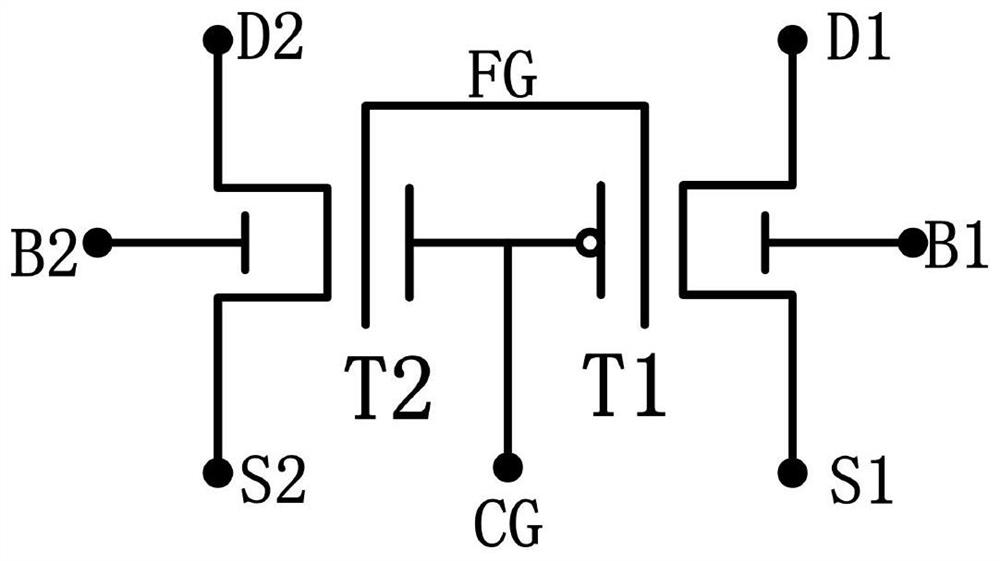
[0037] The present invention provides a structure of a floating gate type FLASH synapse device, which includes a plurality of floating gate type FLASH synapse device units. The structure principle is as follows: figure 1 shown. The device of this structure is a 7-terminal device, which respectively includes the source S1, the drain D1, the substrate B1 of the first floating gate MOS transistor, the source S2, the drain D2, the substrate B2 and the control gate CG of the second floating gate MOS transistor; and The first floating gate MOS transistor and the second floating gate MOS transistor share a common control gate CG and a common floating gate FG, and control the electrons on the floating gate through programming and erasing, thereby realizing the multiplication of the first floating gate MOS transistor and the second floating gate MOS transistor. A state of storage information. Specifically, the floating gate type FLASH synapse device unit of the present invention is co...

Embodiment 2

[0047] The invention provides a preparation method of a floating gate type FLASH synapse device structure, comprising:

[0048] A silicon base is provided as the substrate 00, and the required deep N well 01, high voltage P well 02, STI isolation trench 03, T1 active region 11 and T2 active region 22 are sequentially fabricated on the substrate 00; the STI The depth of the isolation groove 03 is The isolation between the T1 and T2 active regions is achieved through the STI isolation trench 03;

[0049] According to the industry standard CMOS process, a sacrificial oxide layer is formed on the substrate 00, and the T1 active region 11 and the T2 active region 22 are subjected to channel modulation lithography and implantation to achieve different intrinsic threshold voltages of T1 and T2;

[0050] Using the above-mentioned surface as the substrate, wet removal of the sacrificial oxide layer to grow a tunnel oxide layer 04; cover the above-mentioned surface with an N-type poly...


PUM


Abstract

The invention discloses a floating gate type FLASH synaptic device structure and a preparation method thereof, belonging to the technical field of microelectronic integrated circuits. The floating gate type FLASH synapse device unit includes two FLASH tubes with common floating gates and common control gates: one pFLASH tube T1 and one nFLASH tube T2; the pFLASH tube T1 and the nFLASH tube T2 are controlled by a common gate method The pFLASH tube T1 and the nFLASH tube T2 store various information states to establish the STDP learning function of T1 and T2, and realize the basic functions of LTD and LTP of the FLASH synapse device. The invention realizes the change of the floating gate charge on the channel resistance based on the common floating gate and the shared charge technology, which can then be converted into the weight relationship between the programming time pulse and the on-resistance or the read current, so as to realize the LTP and the reading current of the synaptic device. LTD function. The device has the characteristics of low power consumption, short programming time, multi-resistance distribution area, structure and process compatible with CMOS, simple steps, safety and reliability, and has broad application prospects in artificial neural network applications.

Description

technical field [0001] The invention relates to the technical field of microelectronic integrated circuits, in particular to a structure of a floating gate type FLASH synapse device for artificial intelligence neuromorphic chips and a preparation method thereof. Background technique [0002] Neurons are the basic unit of information processing in the brain, and synapses are the functionally connected parts between neurons, which means that the impulses of one neuron are transmitted to another neuron or to another cell in contact with each other. Structure is a key part of information transmission and processing; its artificially constructed synapses are widely considered to be the core components of hardware-based brain-like computers and artificial intelligence systems. At present, the types of artificial synapse devices mainly include double-terminal synapse devices and multi-terminal synapse devices. The former includes resistor synapse devices (resistive memory and phase...

Claims


Application Information

Patent Timeline
Patent Type & Authority Patents(China)
IPC IPC(8): H01L27/1156H01L27/11519H01L27/11521
CPCH10B41/10H10B41/70H10B41/30
Inventor 刘国柱魏敬和于宗光宋思德曹利超赵伟
Owner 58TH RES INST OF CETC
Why Eureka
Eureka Blog
Learn More