

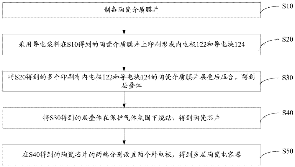
Manufacturing method for multi-layer ceramic capacitor
A technology of multilayer ceramics and manufacturing methods, applied in the direction of laminated capacitors, fixed capacitor parts, etc., can solve problems such as large static electricity and increased scrap rate
- Summary
- Abstract
- Description
- Claims
- Application Information
AI Technical Summary
Problems solved by technology
Method used
Image

Examples
Embodiment 1
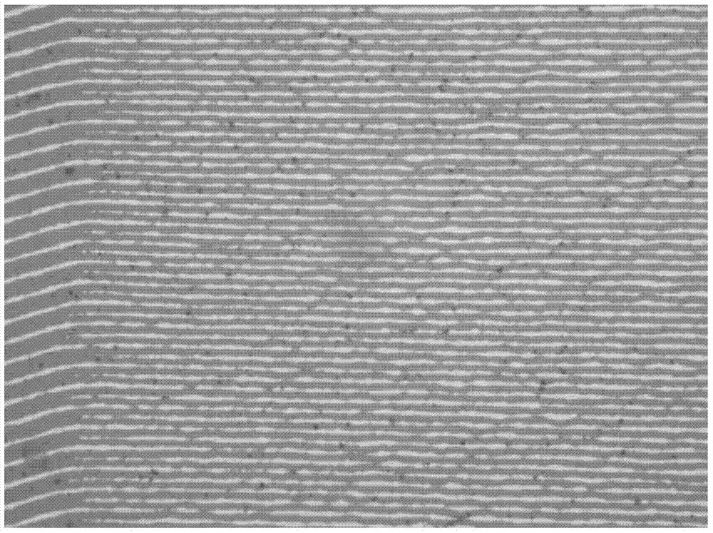
[0060] Mix 4000g of barium titanate ceramic powder, 1500g of polyvinyl butyral, and 3500g of toluene and ethanol in a mass ratio of 1:1 to obtain a ceramic slurry, and then cast the ceramic slurry A rectangular ceramic dielectric membrane with a thickness of 3 μm was obtained by casting.
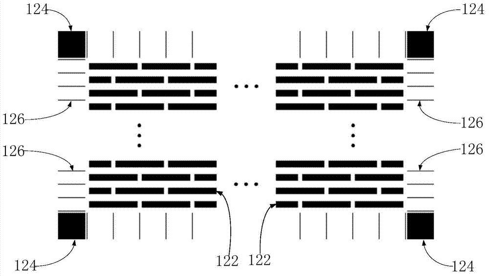
[0061] The nickel paste is used to print on the ceramic dielectric membrane to form internal electrodes, conductive blocks and dividing lines. The internal electrode is arranged in the middle of the ceramic dielectric diaphragm, and the four conductive blocks are respectively arranged on the four corners of the rectangular ceramic dielectric diaphragm. The thickness of the inner electrode and the conductive block are both 1μm, and the area of each conductive block is 50mm 2 .
[0062] Laminate 180 ceramic dielectric membranes printed with internal electrodes and conductive blocks, press them together under hydrostatic pressure, and divide vertically and horizontally according to the divi...
PUM
| Property | Measurement | Unit |
|---|---|---|
| Thickness | aaaaa | aaaaa |
| Area | aaaaa | aaaaa |
| Thickness | aaaaa | aaaaa |
Abstract
Description
Claims
Application Information