

Manufacturing method for semiconductor device
A manufacturing method and semiconductor technology, applied in semiconductor/solid-state device manufacturing, electrical components, circuits, etc., can solve problems such as low production efficiency, complicated manufacturing process, and complicated manufacturing technology, and achieve the effect of accurate dimensions
- Summary
- Abstract
- Description
- Claims
- Application Information
AI Technical Summary
Problems solved by technology
Method used
Image

Examples
Embodiment Construction
[0026] In order to make the object, technical solution and advantages of the present invention clearer, the present invention will be further described in detail below with reference to the accompanying drawings and examples.
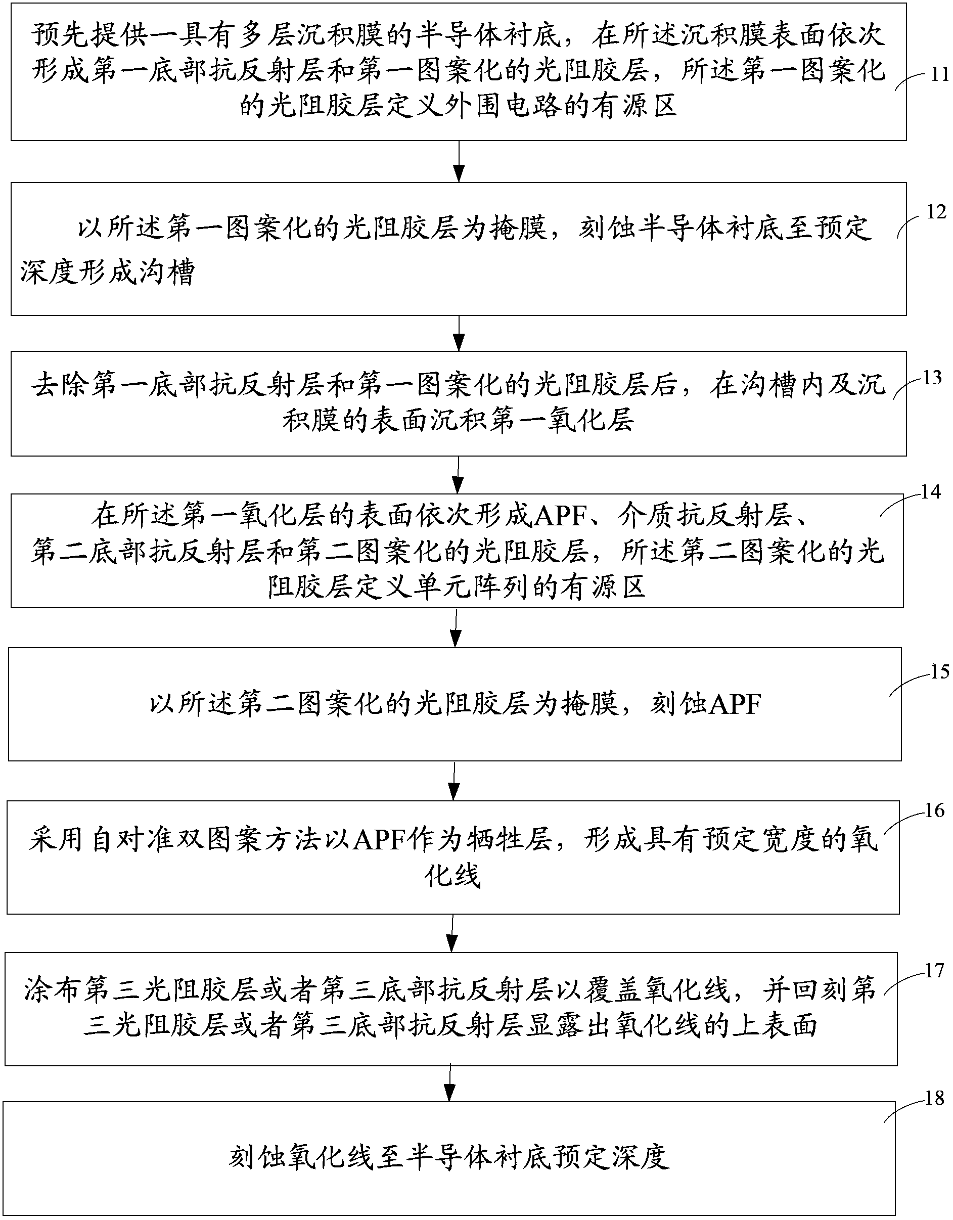
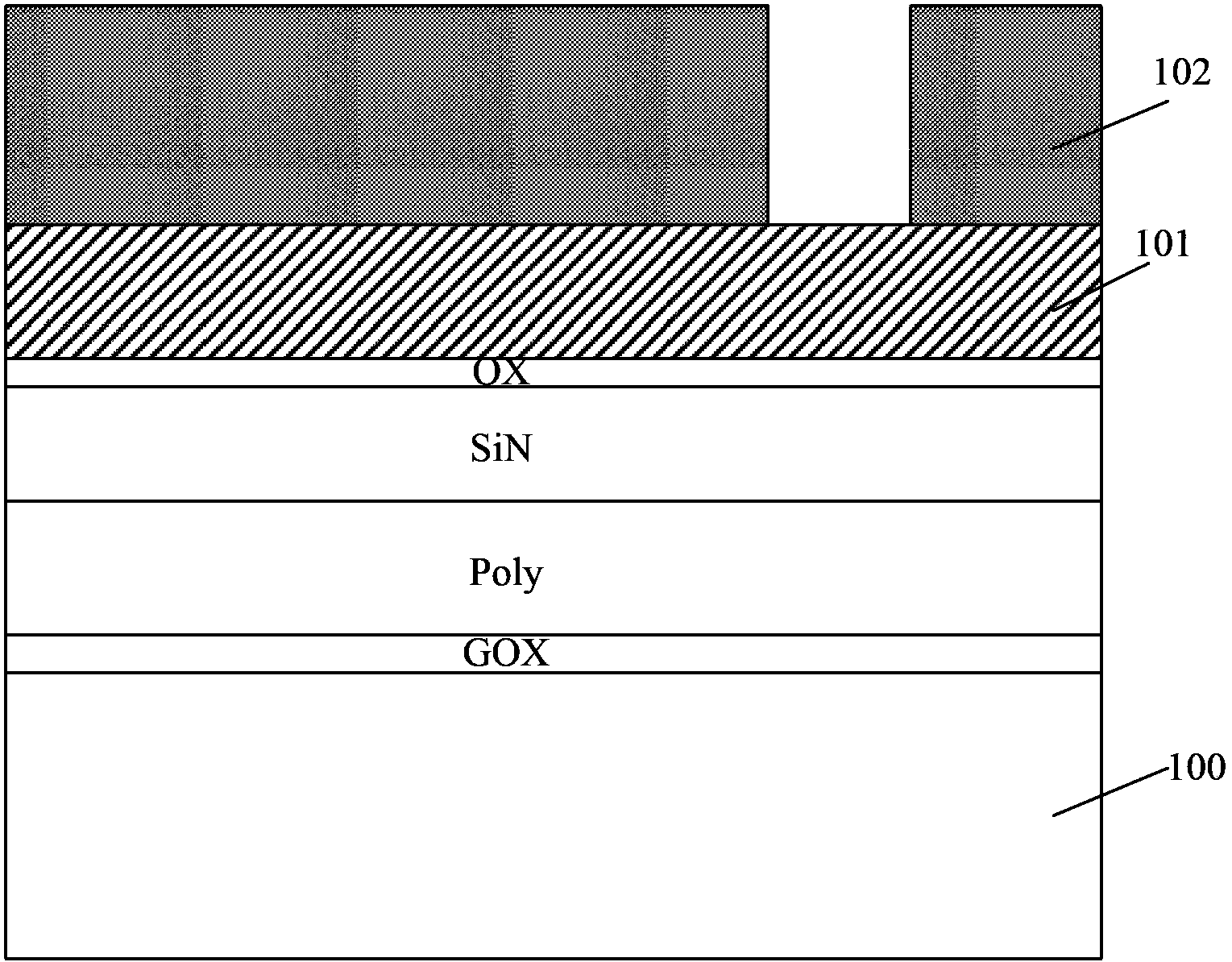
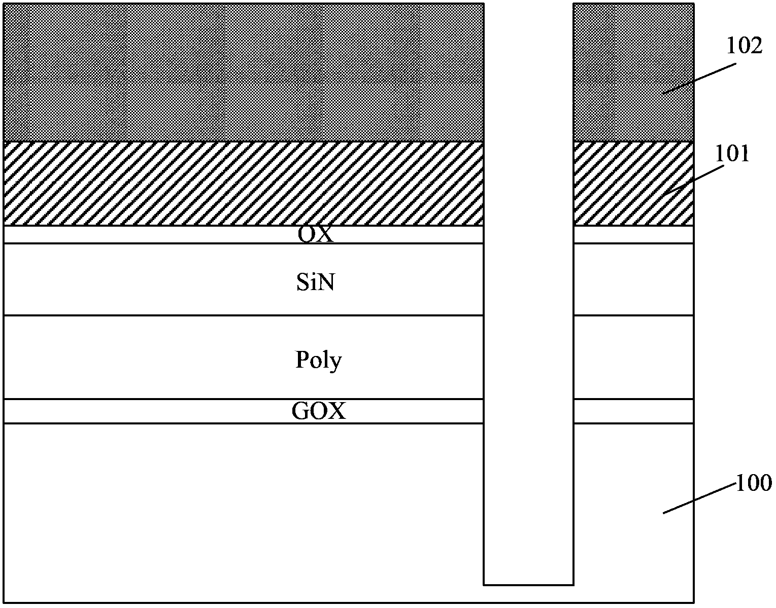
[0027] The schematic flow chart of the manufacturing method of the semiconductor device of the present invention is as figure 1 As shown, it includes the following steps, which are combined below Figure 2a to Figure 2i Be explained.
[0028] Step 11, see Figure 2a , providing a semiconductor substrate 100 with a multi-layer deposited film in advance, forming a first bottom anti-reflection layer 101 and a first patterned photoresist layer 102 sequentially on the surface of the deposited film, and the first patterned photoresist layer 102 The resist layer 102 defines the active area of the peripheral circuit;
[0029] Wherein, the multi-layer deposited film sequentially includes a gate oxide layer (GOX), a polysilicon layer (poly), a silicon nitrid...
PUM
 Abstract
Description
Claims
Application Information