Packaging-free UVLED solidification light source module

A light source module and LED chip technology, which is applied in the direction of electric solid-state devices, electrical components, circuits, etc., can solve the problems of limited radiant energy of a single LED, energy density that cannot meet the needs of curing, and high-integration assembly that cannot be achieved.

Inactive Publication Date: 2014-05-14
JIANGSU XINGUANGLIAN TECH
View PDF5 Cites 14 Cited by
  • Summary
  • Abstract
  • Description
  • Claims
  • Application Information

AI Technical Summary

Problems solved by technology

[0002] Most of the traditional UV curing inks and glues use composite light diluents, which require different wavelengths of purple and ultraviolet light to achieve good curing. LEDs can only emit light of a single wavelength, and the radiant energy of a single LED is limited. Traditional packaging methods cannot achieve high Integrated assembly, the energy density cannot meet the needs of traditional UV ink and glue photocuring

Method used


Image

  • Packaging-free UVLED solidification light source module
  • Packaging-free UVLED solidification light source module
  • Packaging-free UVLED solidification light source module

Examples


Embodiment Construction

[0012] The present invention will be further described below in conjunction with specific drawings.

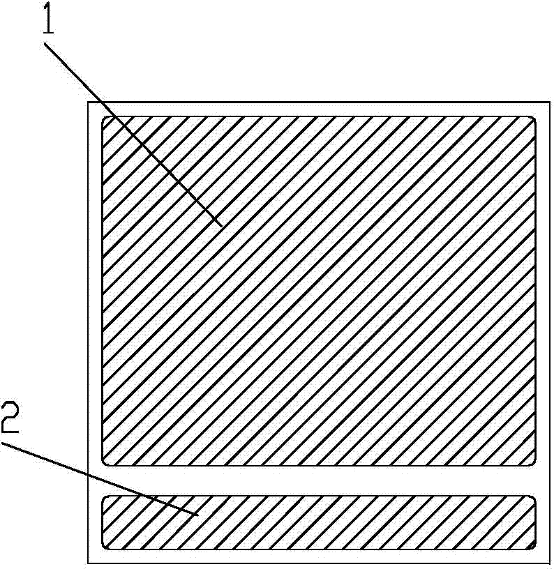
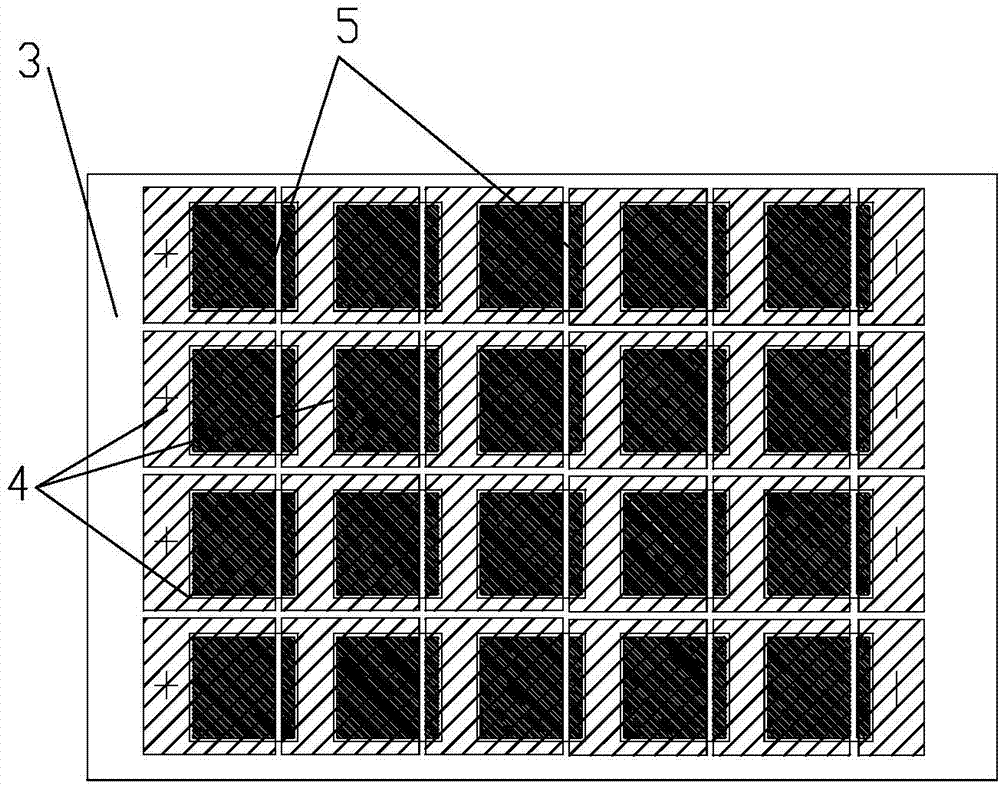
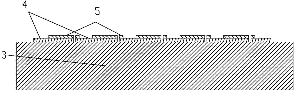
[0013] Such as Figure 1 ~ Figure 4 As shown: the package-free UVLED curing light source module includes P eutectic electrode 1, N eutectic electrode 2, silicon substrate 3, reflective interconnection layer 4, positive and negative eutectic layer 5, LED chip 6, potting glue 7, Water cooling radiator 8, water inlet pipe 9, water outlet pipe 10, welding layer 11, etc.

[0014] Such as Figure 4 As shown, the package-free UVLED curing light source module of the present invention includes a silicon substrate 3, a reflective interconnection layer 4 is provided on the front surface of the silicon substrate 3, and several groups of positive and negative eutectic layers 5 are provided on the upper surface of the reflective interconnection layer 4, each Both the positive and negative eutectic layers 5 are composed of a P eutectic electrode 1 and an N eutectic electrode 2. An LED chip 6 is ...


PUM


Abstract

The invention relates to a packaging-free UVLED solidification light source module which comprises a silicon substrate. The packaging-free UVLED solidification light source module is characterized in that the front face of the silicon substrate is provided with a reflecting interconnection layer, and the upper surface of the reflecting interconnection layer is provided with a plurality of sets of positive and negative eutectic layers which are composed of P eutectic electrodes and N eutectic electrodes and provided with LED chips; the surfaces of the LED chips are covered with pouring sealants, and the LED chips are formed by integrating the LED chips with four wavelengths of 365 nm, 380 nm, 395 nm and 405 nm according to a ratio of 1:1:1:1; the back face of the silicon substrate is connected with a water cooling radiator through a welding layer, and the water cooling radiator is provided with a water inlet pipe and a water outlet pipe. Due to driving currents of the chips with the different wavelengths, the requirements for solidification wavelength and energy ratio of the majority of UV ink and glue can be met, the test heat resistance coefficient of the test light source module is lower than 3 DEG C/W, and the maximum driving power of the single LED chip can reach 5 W.

Description

Technical field [0001] The invention relates to a packaging-free UVLED curing light source module, which belongs to the technical field of semiconductor packaging. Background technique [0002] Traditional UV curing inks and glues mostly use composite light diluents, which require different wavelengths of violet and ultraviolet light to achieve good curing. LEDs can only emit light of a single wavelength, and the radiation energy of a single LED is limited, and traditional packaging methods cannot achieve high With integrated assembly, the energy density cannot meet the requirements of traditional UV ink and glue photocuring. Summary of the invention [0003] The purpose of the present invention is to overcome the deficiencies in the prior art and provide a package-free UVLED curing light source module, which achieves high integration and ultra-low thermal resistance. [0004] According to the technical solution provided by the present invention, the package-free UVLED curing light...

Claims


Application Information

Patent Timeline
Patent Type & Authority Applications(China)
IPC IPC(8): H01L25/075H01L33/62H01L33/64
Inventor 黄慧诗郭文平柯志杰邓群雄
Owner JIANGSU XINGUANGLIAN TECH
Why Eureka
Try Eureka