
Cache design method for reducing STT-RAM power consumption by utilizing temperature difference on three-dimensional integrated circuit chip

A technology of an integrated circuit and a design method, applied in the design field of magnetic tunnel junction power consumption, can solve the problems of large write power consumption and large write delay, reduce write power consumption, improve performance, optimize write current and write effect of time

Active Publication Date: 2014-05-21
BEIHANG UNIV
View PDF5 Cites 22 Cited by
  • Summary
  • Abstract
  • Description
  • Claims
  • Application Information

AI Technical Summary

Problems solved by technology

If STT-RAM is simply used for on-chip cache, it will result in very large write power consumption and write delay, which may offset the benefits of using STT-RAM

Method used


Image

  • Cache design method for reducing STT-RAM power consumption by utilizing temperature difference on three-dimensional integrated circuit chip
  • Cache design method for reducing STT-RAM power consumption by utilizing temperature difference on three-dimensional integrated circuit chip
  • Cache design method for reducing STT-RAM power consumption by utilizing temperature difference on three-dimensional integrated circuit chip

Examples


Embodiment Construction

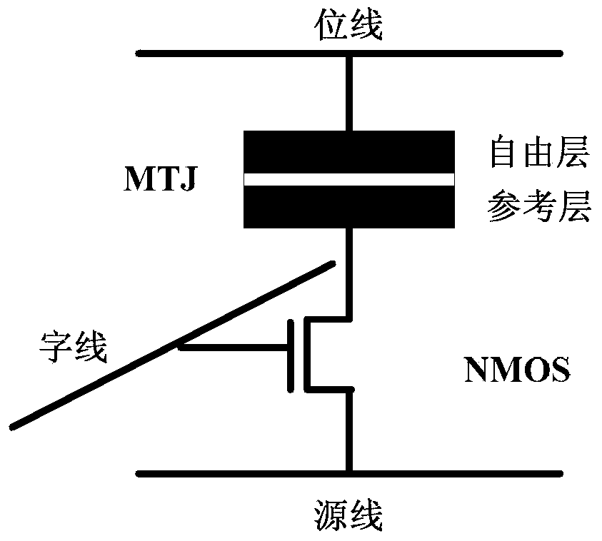
[0027] The working principle of the STT-RAM storage unit involved in the present invention is as follows: figure 1 shown. STT-RAM storage unit generally adopts 1T1J (1Transistor and 1MTJ). Transistors control access to MTJ data. The structure of MTJ is divided into free layer, reference layer and intermediate oxide layer. Wherein the magnetization direction of the reference layer is fixed. By applying currents in different directions to the MTJ, the magnetization direction of the free layer can be changed. If the magnetization direction of the free layer is the same as that of the reference layer, the resistance value of the MTJ becomes smaller, and it can be regarded as storing logic "0". Otherwise, a logic "1" is stored. When reading the data of the memory cell, the word line is set to be valid, and all small voltages of 0.1V are applied between the bit line BL and the source line SL. According to the similarities and differences of the magnetization directions of the ...


PUM


Abstract

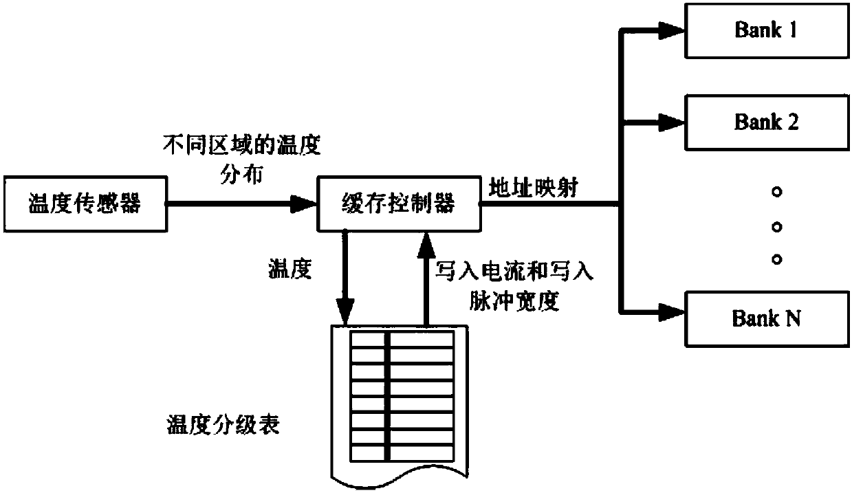
The invention provides a cache design method for reducing STT-RAM power consumption by utilizing temperature difference on a three-dimensional integrated circuit chip. The method includes the first step of modifying cache controller design, the second step of carrying out discretization on temperature difference grades, dividing a Cache Bank into a plurality of areas according to the temperature difference, and adopting different currents to write in the different areas, and carrying out reasonable grading on the Cache Bank located in the different temperature areas according to write-in time difference, the third step of modifying an STT-RAM read-write circuit and selecting different write-in current intensities and write-in pulse intensities according to the temperature difference of the Bank, and the fourth step of designing a buffer mechanism, solving the problem that migration rates are unmatched due to the temperature difference of the source Bank and the target Bank in the data migration process, and avoiding reduction of the data migration performance because of the difference of write performance of the source Bank and the write performance of the target Bank in the data migration process. The cache design method has practical value in the technical field of nonvolatile memories.

Description

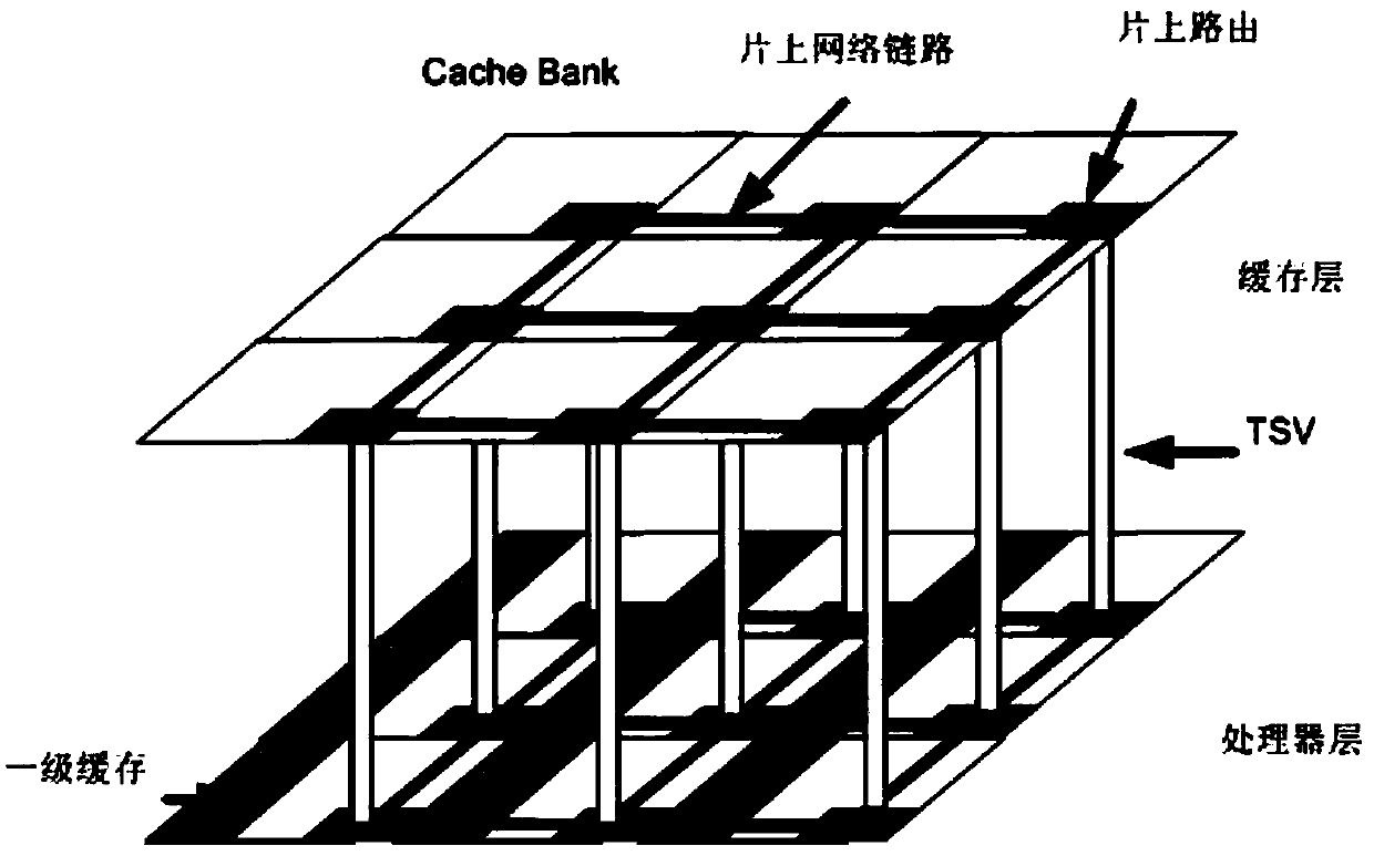
technical field [0001] The invention relates to a buffer design method for reducing power consumption of STT-RAM by using temperature difference on a three-dimensional integrated circuit chip. It uses STT-RAM storage devices to replace traditional SRAM devices as chip buffers. According to the magnetic tunnel junction (MTJ) write current According to the relationship with temperature, a design method to reduce the power consumption of STT-RAM cache (Cache) by using the temperature difference on the chip is proposed. The invention belongs to the technical field of nonvolatile memory design. Background technique [0002] With the continuous improvement of process size, the integration level of on-chip transistors is getting higher and higher. In order to greatly improve the performance of processors under a given power consumption constraint, multi-core processors are widely used. For example, IBM Power7, Intel's Core series processors and Tilera's Tile-GX series processors....

Claims


Application Information

Patent Timeline
Patent Type & Authority Applications(China)
IPC IPC(8): G06F12/08G11C11/16G06F3/06
CPCG11C11/1653G11C11/1675G11C11/1693
Inventor 成元庆郭玮赵巍胜张有光
Owner BEIHANG UNIV
Learn More