FeS2 film and preparation method thereof

A thin film and seed layer technology, which is applied in the direction of final product manufacturing, sustainable manufacturing/processing, photovoltaic power generation, etc., can solve the problems of low photoelectric conversion efficiency and poor light absorption performance, so as to increase the effective light absorption area and improve photoelectricity. Conversion efficiency and the effect of simple synthesis conditions

Inactive Publication Date: 2014-05-28
ZHEJIANG UNIV
View PDF8 Cites 10 Cited by
  • Summary
  • Abstract
  • Description
  • Claims
  • Application Information

AI Technical Summary

Problems solved by technology

[0006] In order to overcome the shortcomings of poor light absorption performance and low photoelectric conversion efficiency of the existing iron disulfide film, the present invention provides a method to improve the light absorption performance and photoelectric conversion efficiency of the iron disulfide film by increasing the effective light absorption area. Iron disulfide nanorod array thin film with conversion efficiency and preparation method thereof

Method used


Image

  • FeS2 film and preparation method thereof
  • FeS2 film and preparation method thereof
  • FeS2 film and preparation method thereof

Examples


Embodiment 1

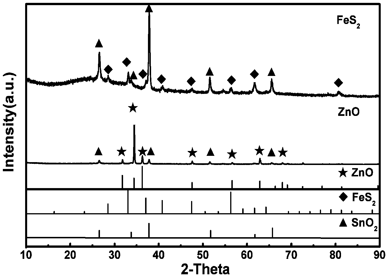
[0039] combined with Figure 1-6 , to further illustrate the present invention:

[0040] a FeS 2 The preparation method of thin film, comprises the following steps:

[0041] 1) Substrate pretreatment: In this example, the size is The conductive glass is used as the substrate, but the size of the substrate is not limited to the example of this embodiment. The substrate was ultrasonically cleaned in acetone solution for 15 minutes, then ultrasonically cleaned in absolute ethanol for 15 minutes, and finally ultrasonically cleaned in deionized water for 15 minutes; the cleaned substrate was dried in a constant temperature drying oven at 100°C, and the dried Base spare;

[0042] 2) Add 0.05mol of zinc acetate dihydrate to the beaker, dissolve it with 50ml of ethylene glycol methyl ether, add 3ml of ethanolamine, and stir at a constant temperature of 60°C for 30 minutes until completely dissolved, forming a uniform and transparent seed layer solution; magnetic stirring The pur...

Embodiment 2

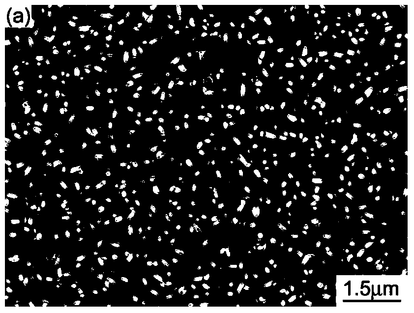
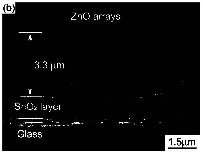
[0051] As shown in Figure 4, a FeS 2 Thin films, including FTO conductive glass substrates covered with FeS 2 array of nanorods, each FeS 2 Nanorods made of FeS 2 accumulation of nanoparticles.

[0052] by FeS 2 One-dimensional ordered FeS composed of nanoparticles 2 The nanorod array structure makes FeS 2 The film has a three-dimensional structure, and the effective light absorption area not only contains FeS 2 the top surface of the nanorods, and includes FeS 2 The outer faces of the nanorods make the FeS 2 The effective light absorption area of ​​the film is much larger than the surface area of ​​the substrate, which can improve the FeS 2 The effective light absorption area of ​​the film has the advantage of improving the light absorption conversion efficiency.


PUM

PropertyMeasurementUnit
thicknessaaaaaaaaaa
electrical resistanceaaaaaaaaaa
thicknessaaaaaaaaaa

Abstract

The invention discloses a preparation method of a FeS2 film. The method comprises the following steps: using FTO conductive glass as a base; configuring a seed layer solution; soaking the base into the seed layer solution to coat in a pulling manner at room temperature; forming a layer of even ZnO nanocrystalline seed on the surface of the base; preparing a precursor solution; forming an even and compact ZnO nano rod array film on the surface of the base; covering the surface of the base with a Fe(OH)3 nano rod array by the ZnO nano rod array film at room temperature; carrying out vulcanizing treatment, and converting the Fe(OH)3 nano rod array into an FeS2 nano rod array. The FeS2 film comprises the base made of the FTO conductive glass; the base is covered with the FeS2 nano rod array; each FeS2 nano rod is formed by stacking FeS2 nano particles. The FeS2 film has the advantages that the optical absorption properties and the photoelectric conversion efficiency are improved by increasing the effective optical absorption area of a ferrous disulfide film.

Description

technical field [0001] The invention relates to the field of photoelectric materials and new energy technologies, in particular to a FeS 2 Thin films and methods for their preparation. technical background [0002] With the outbreak of the economic crisis in 2008 and the intensification of Sino-US photovoltaic trade frictions, the development of the global photovoltaic industry has slowed down and faced a serious crisis, causing most photovoltaic companies to go bankrupt or bear heavy economic burdens. The root cause is cost. Therefore, cost reduction is an important factor that must be considered for any solar material. At this stage, the conversion efficiency of crystalline silicon solar cells is undoubtedly the highest, and it still occupies a dominant position in large-scale applications and industrial production. However, the high cost of raw silicon and the scarcity of resources have limited the future development of silicon solar cells, and at the same time, compou...

Claims


Application Information

Patent Timeline
Patent Type & Authority Applications(China)
IPC IPC(8): H01L31/20H01L31/0296
CPCH01L31/0296H01L31/1836Y02E10/50Y02P70/50
Inventor 汪牡丹刘嘉斌黄六一孟亮
Owner ZHEJIANG UNIV
Why Eureka
Try Eureka