Structure for monitoring etching back depth and monitoring method
A deep, wafer technology, used in electrical components, circuits, semiconductor/solid-state device testing/measurement, etc., can solve the problems of increasing the initial cost of testing, expensive stepper, large maintenance cost, etc., to achieve cost reduction, better Practical, accurate results
- Summary
- Abstract
- Description
- Claims
- Application Information
AI Technical Summary
Problems solved by technology
Method used
Image
Examples
Embodiment Construction
[0037] As mentioned in the background, the existing monitoring methods for polysilicon etch-back depth of trench DMOS devices are either to perform destructive testing on wafer chips, or to use expensive instruments for testing, both of which are costly , The monitoring method is too complicated and other defects, so it cannot meet the requirements of assembly line production.
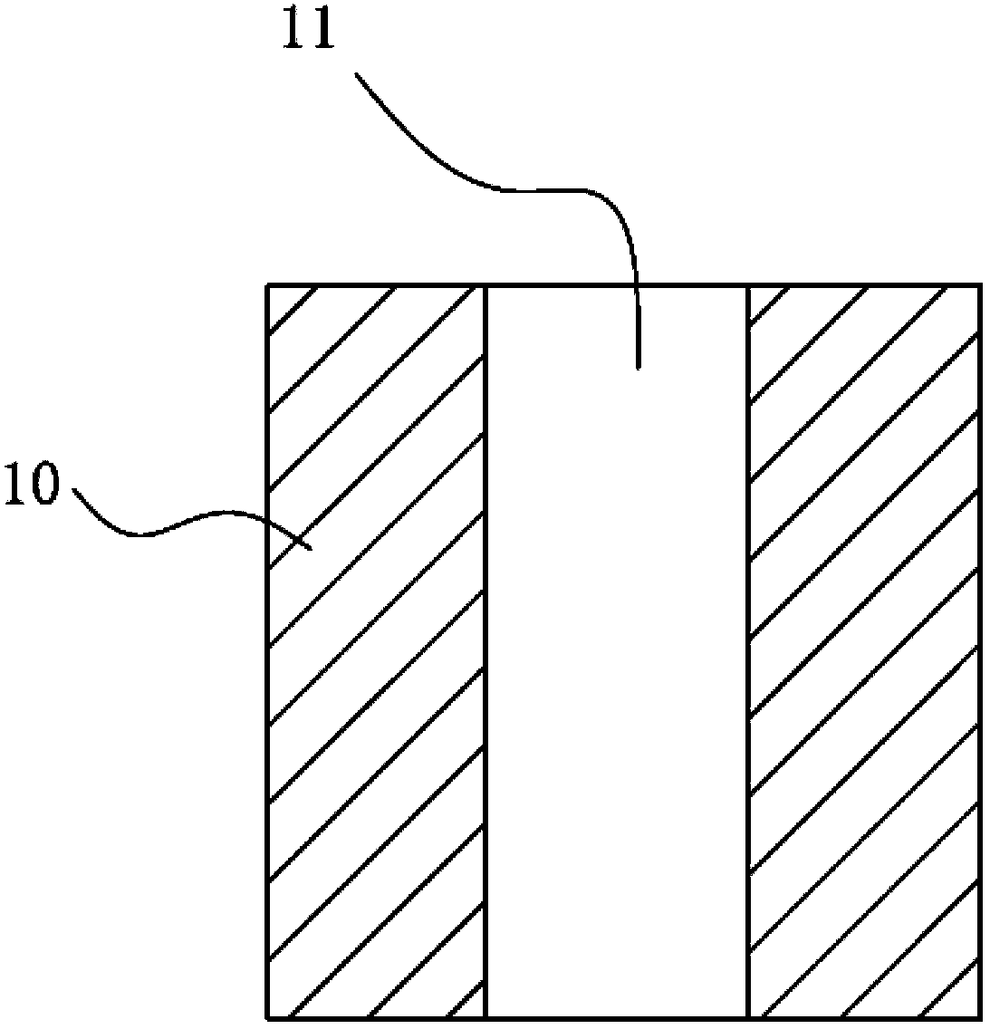
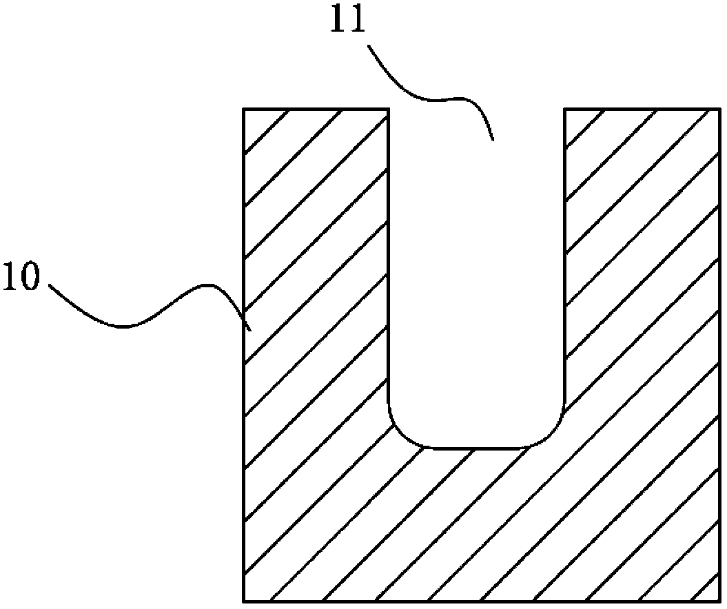
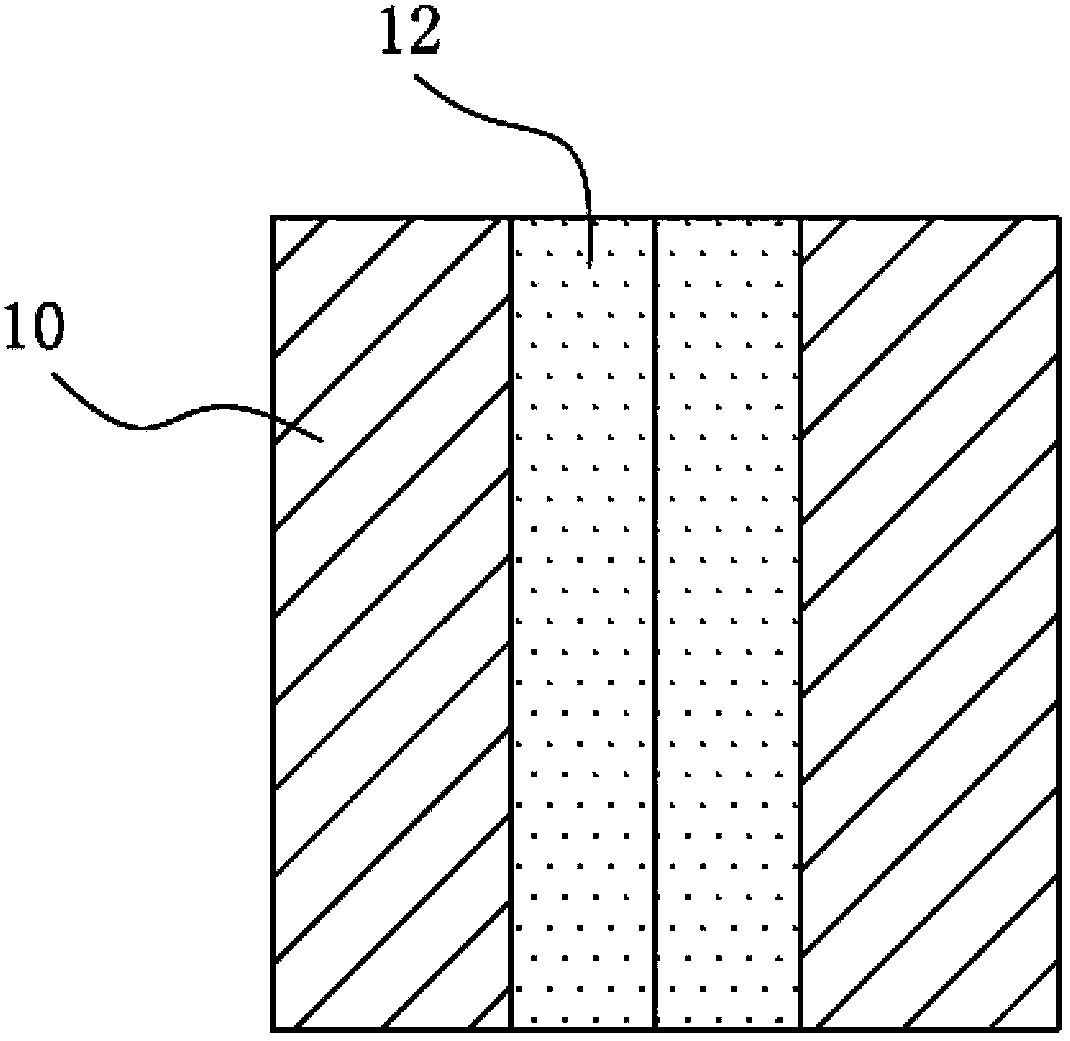
[0038] Therefore, aiming at the defects in the prior art, the present invention proposes a monitoring structure and method for engraving back depth. The monitoring structure is made in the non-element area of the wafer substrate, and is a groove with a special structure. After the groove undergoes a polysilicon etching process, the polysilicon can be divided into a blank area and a filling area in the groove. And at the junction of the two regions, an obvious polysilicon inflection point appears. Using the position where the inflection point appears in the monitoring structure, the corresponding etc...
PUM
 Abstract
Description
Claims
Application Information


