LED (light-emitting diode) packaging method
A transparent encapsulation, half-etching technology, applied in electrical components, circuits, semiconductor devices, etc., can solve the problems of low reliability of LEDs, and achieve the effect of increasing difficulty, high reliability and low packaging cost
- Summary
- Abstract
- Description
- Claims
- Application Information
AI Technical Summary
Problems solved by technology
Method used
Image
Examples
Embodiment Construction
[0026] In order to make the object, technical solution and advantages of the present invention clearer, the present invention will be further described in detail below in conjunction with the accompanying drawings and embodiments. It should be understood that the specific embodiments described here are only used to explain the present invention, not to limit the present invention.
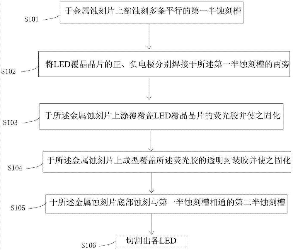
[0027] In the embodiment of the present invention, a plurality of parallel first half-etched grooves are etched on the upper part of the metal etching sheet, and then the positive and negative electrodes of the LED flip chip are respectively welded to both sides of the first half-etched grooves, and then the metal Coat the fluorescent glue covering the LED flip chip on the etched sheet and let it solidify, then form the transparent silica gel covering the fluorescent glue on the metal etched sheet and let it solidify, and then etch the bottom of the metal etched sheet with the first The half-etched...
PUM
 Abstract
Description
Claims
Application Information


