Dielectric film current limiting type vertical cavity surface emitting laser and manufacturing method thereof

A technology of vertical cavity surface emission and dielectric thin film, which is applied in the direction of lasers, laser components, semiconductor lasers, etc., can solve the problems of poor performance consistency, low process precision, poor reliability, etc., and achieve consistency, simplified preparation process, high consistent effect

Active Publication Date: 2014-06-18
CHANGCHUN INST OF OPTICS FINE MECHANICS & PHYSICS CHINESE ACAD OF SCI
View PDF7 Cites 11 Cited by
  • Summary
  • Abstract
  • Description
  • Claims
  • Application Information

AI Technical Summary

Problems solved by technology

[0004] The purpose of the present invention is to propose a dielectric thin film current-confined vertical cavity surface emitting laser and its manufacturing method, which solves the problems of low process precision, poor reliability and poor performance consistency in the prior art. The current limiting window with special shape realizes the improvement of multiple performances of the device

Method used


Image

  • Dielectric film current limiting type vertical cavity surface emitting laser and manufacturing method thereof
  • Dielectric film current limiting type vertical cavity surface emitting laser and manufacturing method thereof
  • Dielectric film current limiting type vertical cavity surface emitting laser and manufacturing method thereof

Examples


Embodiment 1

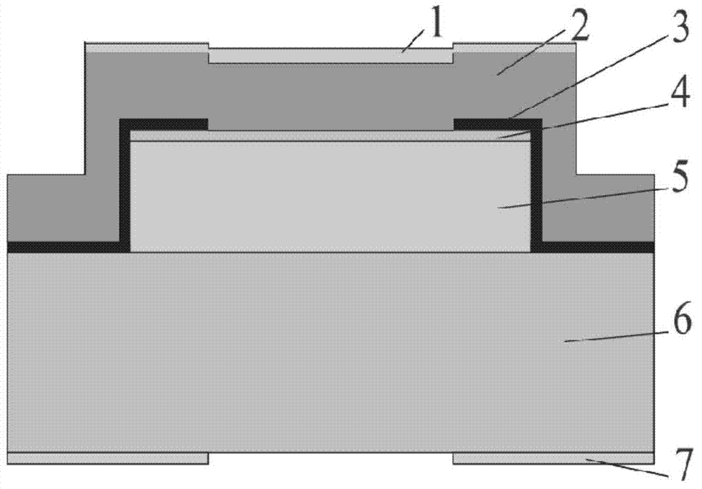
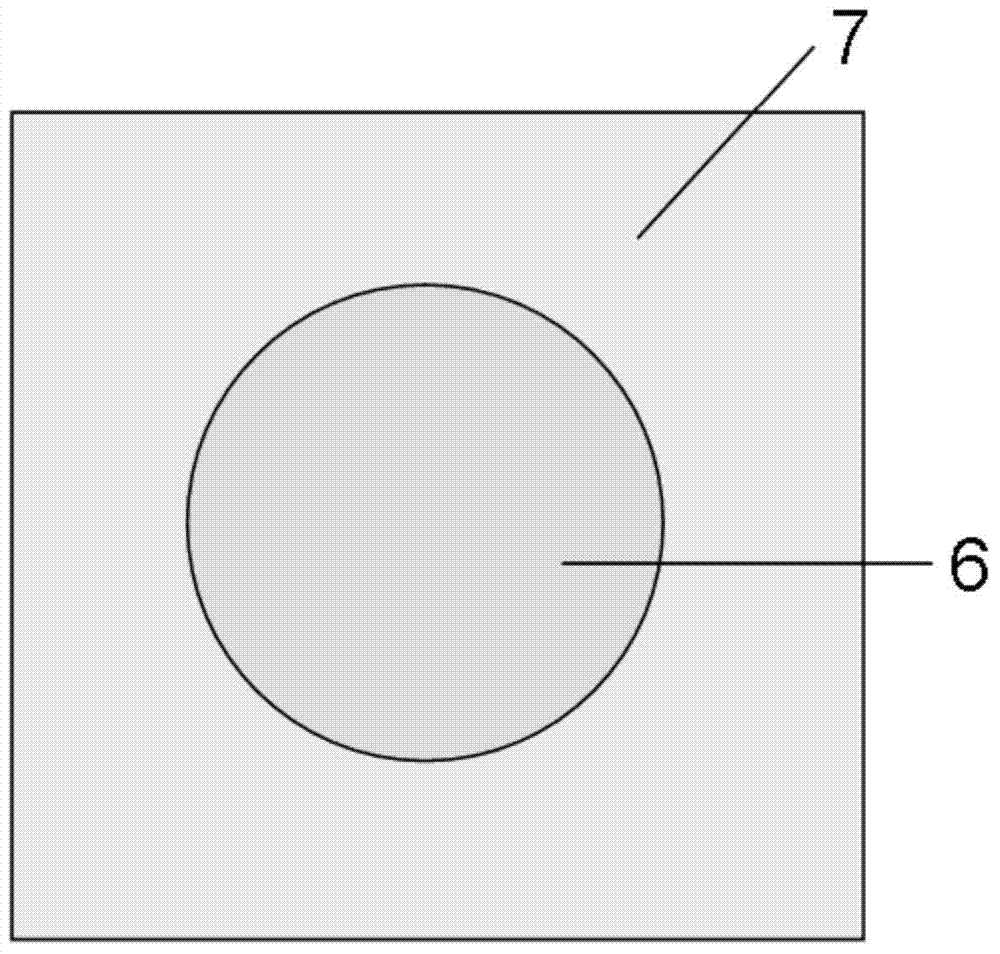
[0044] See attached figure 1 , attached figure 2 And attached image 3 , the dielectric thin film current confinement type vertical cavity surface emitting laser of the present invention comprises:

[0045] A substrate layer 6, the substrate layer 6 is a GaAs structure;

[0046] The N-type DBR layer 5 and the active layer 4 are sequentially grown on the upper end of the substrate layer 6, and the active layer 4 and the N-type DBR layer 5 form a cylindrical mesa;

[0047] Make the dielectric thin film current confinement layer 3 on the upper end of the cylindrical mesa formed by the active layer 4 and the N-type DBR layer 5 and the upper end of the substrate layer 6, and the dielectric thin film current confinement layer 3 on the upper end of the active layer 4 has a A current confinement window through which the active layer 4 is exposed, and the dielectric thin film current confinement layer 3 has a refractive index lower than 2.0 and a thermal conductivity higher than 50...

Embodiment 2

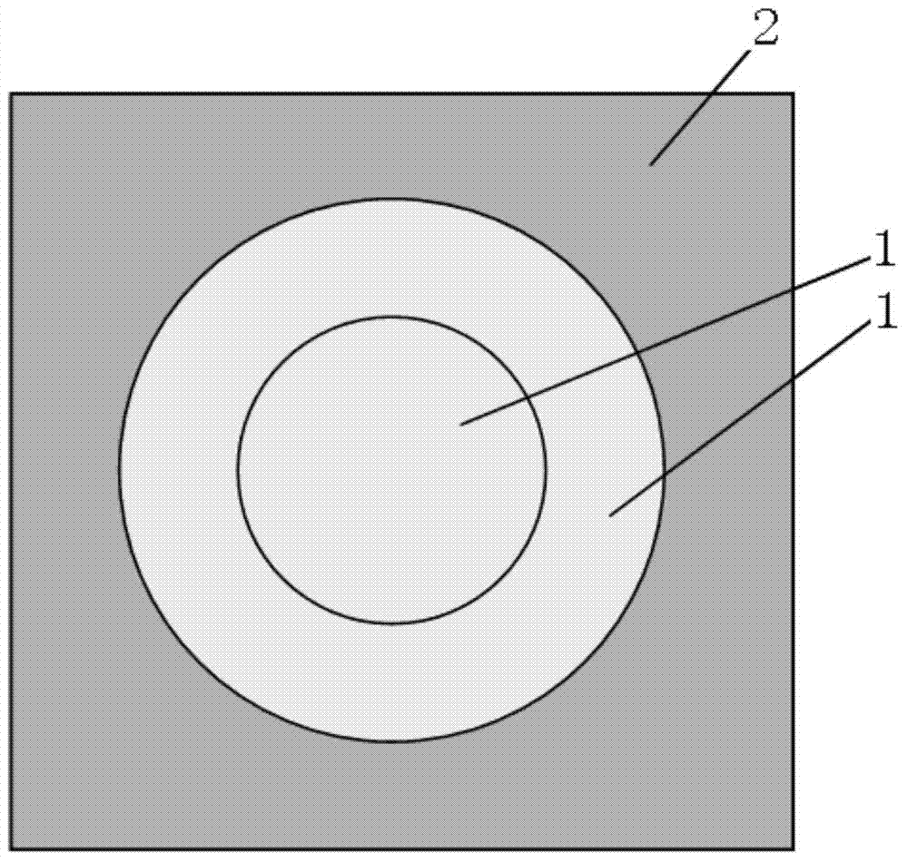
[0071] See attached Figure 5 The difference between the present embodiment and the first embodiment is that the current limiting window and the light output window are both of multiple circular structures.

Embodiment 3

[0073] See attached Figure 6 The difference between the present embodiment and the first embodiment is that the current limiting window and the light output window are polygonal structures.


PUM


Abstract

The invention relates to a dielectric film current limiting type vertical cavity surface emitting laser and a manufacturing method of the emitting laser, belongs to the field of a semiconductor laser, and solves the problems of low process precision, poor reliability and poor performance consistency in the prior art. The dielectric film current limiting type vertical cavity surface emitting laser structurally comprises an N-surface electrode, a substrate layer, an N type DBR layer, an active layer, a dielectric film current limiting layer, a P type DBR layer and a P-surface electrode in arrangement from bottom to top. The method provided by the invention is characterized in that the N type DBR layer and the active layer sequentially grow on the substrate layer, the N type DBR layer and the active layer are etched into a cylindrical table top, in addition, the substrate layer is exposed, the dielectric film current limiting layer grows on the surface of the cylindrical table top and the surface of the substrate layer, a current limiting window is etched at the dielectric film current limiting layer, and in addition, the active layer is exposed; the P type DBR layer grows on the upper surface of the dielectric film current limiting layer and the upper surface of the active layer in an epitaxy way; the P-surface electrode and the N-surface electrode are respectively manufactured on the upper surface of the P type DBR layer and the lower surface of the substrate layer.

Description

technical field [0001] The invention belongs to the technical field of semiconductor lasers, in particular to a dielectric film current-limited vertical cavity surface-emitting laser and a manufacturing method thereof. Background technique [0002] The vertical cavity surface emitting laser was first proposed by Professor K.Iga of Tokyo Institute of Technology in 1979 (Soda, H. et al., Japanese Journal of Applied Physics, vol.18, no.12, 2329-2330), is a Composed of multi-layer semiconductor materials, the optical device that emits laser light from the surface is mainly composed of upper and lower distributed Bragg reflectors and an active area sandwiched in the middle. This laser emits light in a direction perpendicular to the chip surface and can output The circular symmetrical spot is very convenient for two-dimensional integration, and because the length of its resonant cavity is on the order of microns, the dynamic single-mode modulation rate is extremely high. At prese...

Claims


Application Information

Patent Timeline
Patent Type & Authority Applications(China)
IPC IPC(8): H01S5/183H01S5/10
Inventor 张星宁永强张建伟张建秦莉王立军
Owner CHANGCHUN INST OF OPTICS FINE MECHANICS & PHYSICS CHINESE ACAD OF SCI
Why Eureka
Try Eureka