Device and method for detecting defects on surface of solar cell

A solar cell and defect detection technology, applied in the energy field, can solve problems affecting the correctness of results, unstable work, short working life, etc., and achieve the effects of improved detection efficiency and accuracy, simple operation, and reduced labor intensity

Inactive Publication Date: 2014-06-18
天津市鑫鼎源科技发展有限公司
View PDF2 Cites 59 Cited by
  • Summary
  • Abstract
  • Description
  • Claims
  • Application Information

AI Technical Summary

Problems solved by technology

However, this method is only suitable for detecting solar panels with a small size, and is not suitable for detecting solar panels with a large size or amorphous silicon type. Therefore, as an industrial production inspection equipment, its limitations are relatively large
[0005] Due to the strong reflection characteristics of the surface of solar cells, the light source lighting technology has a great influence on the detection of surface defects. The light source used in the past inspection equipment is usually an incandescent lamp, which has a short working life, low light efficiency, unstable work, and stroboscopic phenomenon. ;
[0006] The surface of solar cells has the characteristics of strong texture and regularity. The detection methods used in the past have not classified the specific defects on the surface of solar cells, and cannot effectively distinguish and identify defects including missing corners, cracks and electrodes. Affect the correctness of the test results

Method used


Image

  • Device and method for detecting defects on surface of solar cell
  • Device and method for detecting defects on surface of solar cell
  • Device and method for detecting defects on surface of solar cell

Examples


Embodiment Construction

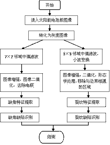
[0035] In order to understand the present invention more clearly, describe the present invention in detail in conjunction with accompanying drawing and embodiment:

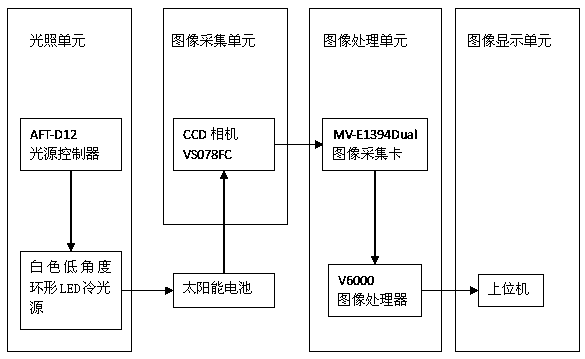
[0036] Solar cell surface defect detection equipment, the circuit includes a lighting unit, an image acquisition unit, an image processing unit, and a display unit. The lighting unit is composed of an AFT-D12 light source controller (DC 12V power adapter) and a white low-angle ring LED cold light source. (Light source controller is 12V DC power supply)

[0037] The image acquisition unit consists of MV-VS078FC CCD camera (maximum resolution 1024X768, 8-bit data output, frame rate 30fps, progressive scanning color CCD), M0814MP lens (image size 2 / 3", minimum object distance 0.1m, Focal length 8mm), MV-E1394Dual image acquisition card (using professional TSB43AB22A dual control chip, high-speed serial real-time data stream transmission, data transmission rate per channel up to 400Mb / s, 6-core interface provides 12V ...


PUM


Abstract

The invention relates to a device and method for detecting defects on the surface of a solar cell. The device comprises a structural member and a detection circuit system. The structural member is composed of a display frame, an observation platform and an installation frame. The detection circuit system comprises an illumination unit, an image collection unit, an image processing unit and a display unit. In the detection process, an unfilled corner defect image is obtained by means of a low-angle annular white LED light source and by conducting image segmentation, wavelet transform and two-dimensional 7*7 pixel field median filtering on an image; for a crack, a defect image of the crack is obtained by conducting two-dimensional median filtering, wavelet transform, image binaryzation, edge detection and morphology operator processing on the image, the detection recognition result is obtained, and the image processing unit finally transmits the processing result to an upper computer of the display unit. The method and the device have the advantages that compared with a manual visual detection and infrared scanning detection method, detection efficiency and detection accuracy are greatly improved, the method is easy to operate and practicable, a large amount of labor force is saved, and the labor intensity is lowered.

Description

technical field [0001] The invention relates to the field of energy, in particular to a solar cell surface defect detection device and method, which are used for detecting defects on the surface of a solar cell panel. Background technique [0002] The surface quality of solar cells is the main factor affecting the power generation efficiency of solar cells, so the surface quality inspection of solar cells has become an indispensable link in the production process. The current detection equipment and methods mainly include: [0003] (1) Manual visual inspection. Manually check the surface quality of the battery board by visual inspection. This method is only suitable for solar cells with obvious surface defects, and it is difficult to detect small defects. Moreover, this method has large human factors and inconsistent defect indicators, making it difficult to adapt to the needs of large-scale industrial production. [0004] (2) Infrared scanning detection. The st...

Claims


Application Information

Patent Timeline
Patent Type & Authority Applications(China)
IPC IPC(8): H02S50/10
CPCY02E10/50
Inventor 隋修武肖金林
Owner 天津市鑫鼎源科技发展有限公司
Why Eureka
Try Eureka