Through silicon via repair circuit

A TSV and circuit technology, applied in the field of chip stacking, can solve problems such as transmission errors and achieve the effect of preventing drift

Inactive Publication Date: 2014-07-02
IND TECH RES INST
View PDF4 Cites 2 Cited by
  • Summary
  • Abstract
  • Description
  • Claims
  • Application Information

AI Technical Summary

Problems solved by technology

However, in 3DIC technology, as long as one of the TSVs is short-circuited with the silicon substrate, the leakage current generated by the power supply voltage will flow into the silicon substrate through the TSV, causing the overall voltage level in the silicon substrate to drift and become unstable. Signals transmitted in TSVs may also be transmitted incorrectly due to voltage level drift of the silicon substrate

Method used


Image

  • Through silicon via repair circuit
  • Through silicon via repair circuit
  • Through silicon via repair circuit

Examples


Embodiment Construction

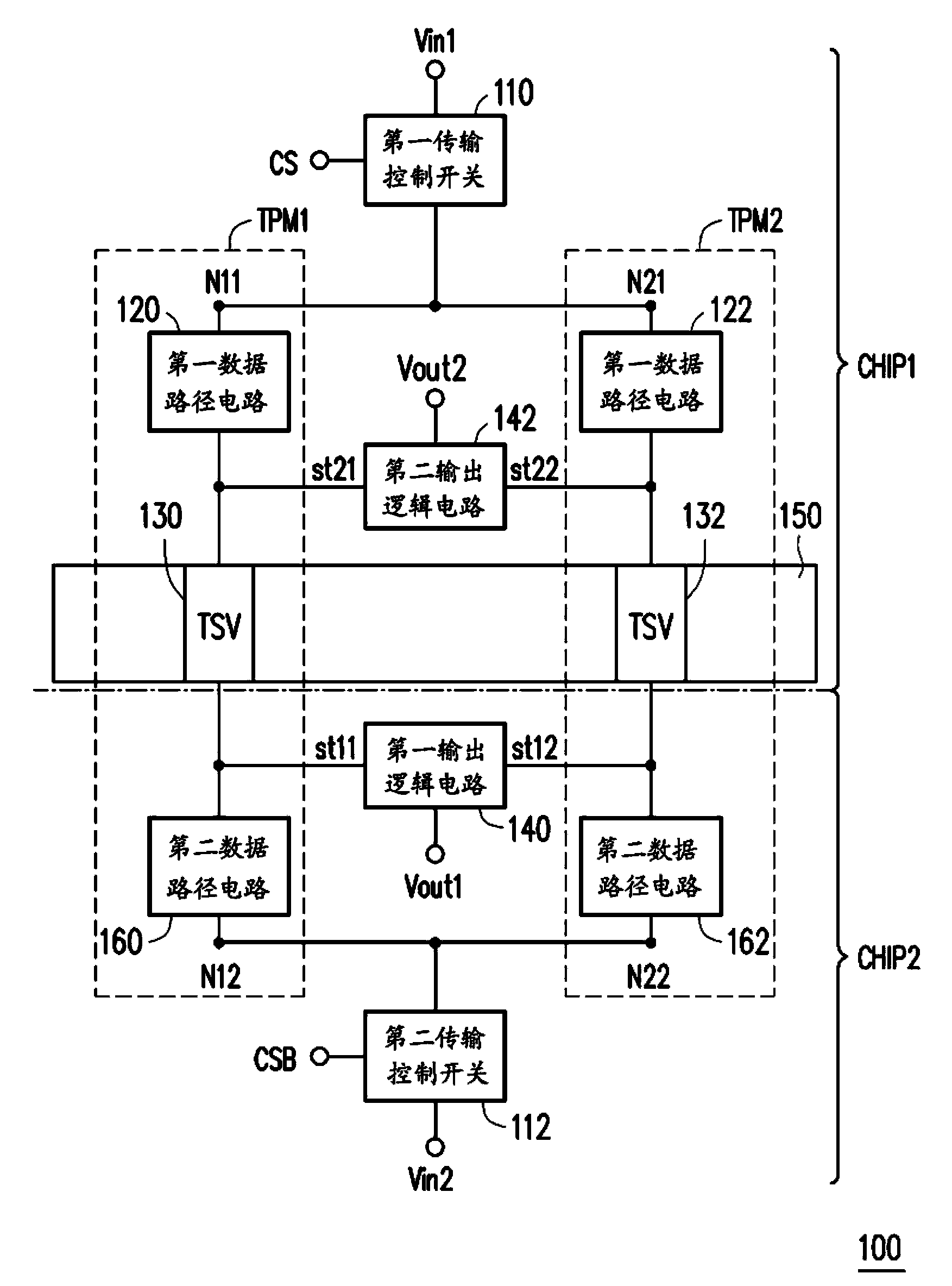
[0075] figure 2 It is a schematic diagram illustrating a TSV repair circuit 100 according to the first embodiment of the present application. Such as figure 2 As shown, the TSV repair circuit 100 that can be used in semiconductor devices includes at least two chips CHIP1, CHIP2 stacked up and down, a first transmission control switch 110 and a second transmission control switch 112, at least two transmission path modules TPM1 and TPM2, the first output logic circuit 140 and the second output logic circuit 142 .

[0076] figure 2 Although it is disclosed that the first chip CHIP1 and the second chip CHIP2 are stacked on top of each other, those who apply the embodiment of the present application should be able to form a semiconductor device (for example, a three-dimensional chip) by stacking a plurality of chips on top of each other, and let two of them think The chips to transmit data are respectively the first chip CHIP1 and the second chip CHIP2, and one or more layers...


PUM


Abstract

A through silicon via (TSV) repair circuit is provided. The TSV repair circuit includes at least two transmission control switches and at least two transmission path modules. Two transmission control switches transmit an input signal of a first chip or a second chip to one of two terminals in each of the transmission path modules according to a switch signal. Each transmission path module includes at least two data path circuits and corresponding TSVs. Each data path circuit includes an input driving circuit, a short-circuit detection circuit and a leakage current cancellation circuit. The short-circuit detection circuit detects whether to detect whether short-circuit on the TSV and a silicon substrate is present and generate a short-circuit detection output signal. The leakage current cancellation circuit to avoid a leakage current generated by a first level voltage to flow into the silicon substrate according to the short-circuit detection output signal.

Description

technical field [0001] The invention relates to a chip stacking technology, and in particular to a through-silicon via (TSV) bidirectional repair circuit of a semiconductor device. Background technique [0002] Since the number of transistors in an integrated circuit (Integrated Circuit; IC) increases continuously, the chip area is increased, making signal delay time (Delay Time) and power consumption (Power Consumption) more serious. In order to improve serious problems such as delay and power consumption, three-dimensional chip (Three Dimension IC; 3DIC) stacking technology is an effective solution that is currently being actively developed. It stacks multiple chips vertically in a three-dimensional space, and different chips The through-silicon via (TSV) structure that penetrates the silicon substrate is used to transmit the signal and power supply voltage to achieve the best benefit of size reduction. [0003] The process technology of 3DIC mainly focuses on three steps...

Claims


Application Information

Patent Timeline
Patent Type & Authority Applications(China)
IPC IPC(8): H01L23/58H01L25/16
CPCH01L23/481H01L25/0657H01L2225/06544H01L2225/06596H01L2924/0002H01L2924/00
Inventor 曾珮玲苏耿立
Owner IND TECH RES INST
Why Eureka
Try Eureka