
Multi-layer hybrid-mode hexagonal substrate integrated waveguide filter

A substrate-integrated waveguide and multi-layer hybrid technology, which is applied to waveguide-type devices, electrical components, circuits, etc., can solve the problem that the filter occupies a large area, and the substrate-integrated waveguide resonator unit area is large, which is not conducive to meeting the requirements of the filter. Issues such as volume, selectivity and integration are strict, to achieve the effect of low loss, small size, and widened stopband width

Inactive Publication Date: 2014-07-02
UNIV OF ELECTRONICS SCI & TECH OF CHINA
View PDF4 Cites 11 Cited by
  • Summary
  • Abstract
  • Description
  • Claims
  • Application Information

AI Technical Summary

Problems solved by technology

With the increasing scarcity of spectrum resources, the requirements for the transmission zero and selectivity of the filter are higher, and in the design of the traditional substrate integrated waveguide filter, the transmission zero obtained by the N-order resonator can only obtain N- 2. If more transmission zeros are required, it can only be achieved by increasing the number of resonant cavities, but the area occupied by the substrate integrated waveguide resonant cavity unit is still relatively large. If the number of resonant cavities increases, the filter It will take up a lot of area in the circuit, which is very unfavorable to meet the stringent requirements of modern communication systems on the volume, selectivity and integration of filters.

Method used


Image

  • Multi-layer hybrid-mode hexagonal substrate integrated waveguide filter
  • Multi-layer hybrid-mode hexagonal substrate integrated waveguide filter
  • Multi-layer hybrid-mode hexagonal substrate integrated waveguide filter

Examples


Embodiment Construction

[0016] The specific embodiments of the present invention will be further described below in conjunction with the accompanying drawings.

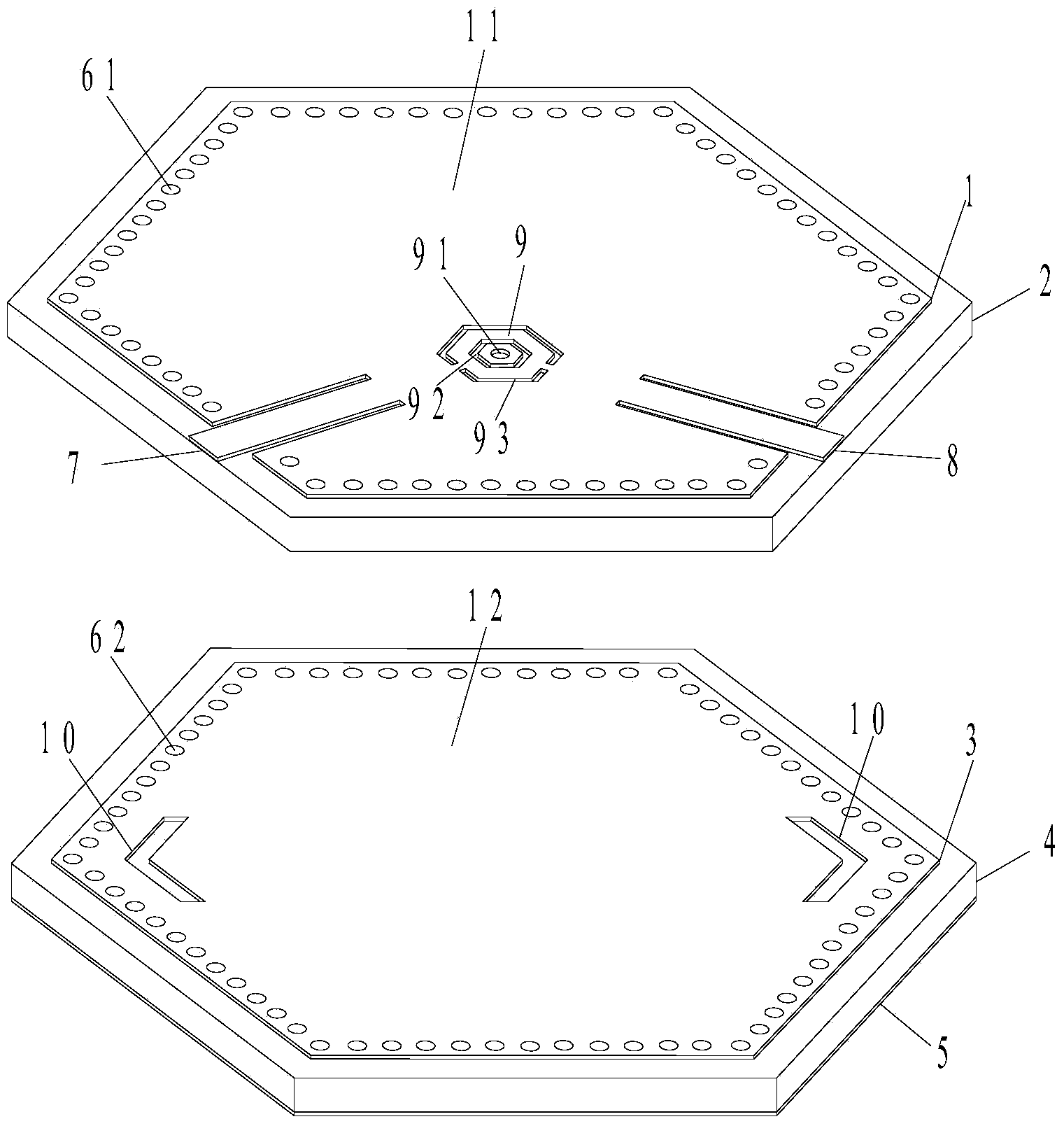
[0017] Such as figure 1 As shown, the multilayer mixed-mode hexagonal substrate integrated waveguide filter includes a first metal layer 1, a first dielectric substrate 2, a second metal layer 3, and a second dielectric substrate 4 stacked in sequence from top to bottom. , the third metal layer 5, the first metal layer 1 is provided with a coplanar waveguide input end 7, a coplanar waveguide output end 8, there is an angle between the coplanar waveguide input end 7 and the coplanar waveguide output end 8 , the first dielectric substrate 2 is provided with an upper metallized through-hole array 61 penetrating the first dielectric substrate 2, and the upper metallized through-hole array 61 is jointly surrounded by the first metal layer 1 and the second metal layer 3 The hexagonal first resonant cavity 11, the second dielectric substrate 4 is ...


PUM


Abstract

The invention discloses a multi-layer hybrid-mode hexagonal substrate integrated waveguide filter which is high in out-of-band selectivity, small in size and low in loss. An included angle is formed between the coplanar waveguide input end and the coplanar waveguide output end of the filter. Due to the loading effect of a hexagonal coupling slot composite structure arranged on a first metal layer, a resonant secondary mode, a left tilted non-resonant higher mode and a right tilted non-resonant higher mode in cavities can be effectively excited, electromagnetic coupling between a filter source and a load can also be excited, and a signal transmission path is effectively increased. In this way, on the basis of an original transmission zero, two transmission zeros are additionally obtained, coupling between a first resonant cavity and a second resonant cavity can be achieved through two symmetrically distributed V-shaped coupling slots formed in a second metal layer, a fourth transmission zero is generated, so that the width of a stop band is increased, and the attenuation of the stop band is increased. Meanwhile, the multi-layer hybrid-mode hexagonal substrate integrated waveguide filter is low in loss and small in size, thereby being suitable for being popularized and applied in the technical field of microwaves and millimeter waves.

Description

technical field [0001] The invention relates to the field of microwave and millimeter wave technology, in particular to a multilayer mixed-mode hexagonal substrate integrated waveguide filter. Background technique [0002] Filter is one of the most commonly used components in communication systems, and its performance directly affects the quality of the circuit system. Traditional filters are generally divided into metal waveguide filters and planar microstrip or stripline structure filters. Traditional metal waveguide filters have the advantages of low loss, high Q value, and good selectivity, but have the disadvantages of large volume, complex processing, and difficulty in integrating with planar circuits. Although microstrip or stripline filters are easy to integrate with planar circuits, they have large losses and low Q values, especially in high-frequency bands, and there is large radiation, which affects circuit stability. [0003] The filter based on the substrate i...

Claims


Application Information

Patent Timeline
IPC IPC(8): H01P1/208
Inventor 徐自强张根郭俊宇夏红程革胜杨邦朝
Owner UNIV OF ELECTRONICS SCI & TECH OF CHINA
Learn More