Silicon-based CMOS image sensor and method of the silicon-based CMOS image sensor for restraining photon-generated carrier surface trap recombination

An image sensor and photo-generated carrier technology, applied in the field of microelectronics, can solve problems such as photo-generated carrier recombination, and achieve the effect of high photo-generated carrier transfer efficiency and low surface trap recombination rate

Inactive Publication Date: 2014-07-09
FUDAN UNIV
View PDF5 Cites 4 Cited by
  • Summary
  • Abstract
  • Description
  • Claims
  • Application Information

AI Technical Summary

Problems solved by technology

However, the carrier collection region of the photodiode is in contact with the surface, which easily causes the recombination of photogenerated carriers in the surface traps.

Method used


Image

  • Silicon-based CMOS image sensor and method of the silicon-based CMOS image sensor for restraining photon-generated carrier surface trap recombination
  • Silicon-based CMOS image sensor and method of the silicon-based CMOS image sensor for restraining photon-generated carrier surface trap recombination
  • Silicon-based CMOS image sensor and method of the silicon-based CMOS image sensor for restraining photon-generated carrier surface trap recombination

Examples


Embodiment Construction

[0029] The present invention will be further described below in conjunction with the accompanying drawings and embodiments.

[0030] The present invention is different from the traditional CMOS image sensor in that the trap suppression layer is formed by implanting two different positions, different energies and different doses, which can be formed by the following methods:

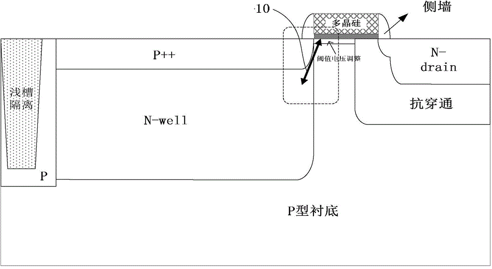
[0031] 1. If Image 6 As shown, after the polysilicon gate is formed, a low-dose P-type ion implantation is performed to form a shallow P-type trap prevention layer in the photosensitive area.

[0032] 2. If Figure 7 As shown, after the first layer of sidewall is formed by sidewall offset technology, a higher dose of P-type ion implantation is performed to form a shallower P+-type trap prevention layer in the photosensitive area.

[0033] 3. If Figure 8 As shown, after the second layer of sidewall deposition is formed, high-dose P-type ion implantation is performed to form a deeper P++-type trap prev...


PUM


Abstract

The invention belongs to the technical field of micro-electronics, and particularly relates to a silicon-based CMOS image sensor and a method of the silicon-based CMOS image sensor for restraining photon-generated carrier surface trap recombination. The silicon-based CMOS image sensor has the advantages of achieving high transfer efficiency of photon-generated carriers and being low in surface recombination rate, and particularly comprises a photodiode (PPD), a floating diffusion region (FD), a transmission transistor (TX), a shallow trench isolation region (STI), an anti-penetration through injection region (APT) and a surface trap restraining layer, wherein the surface trap restraining layer is formed by injecting ions in a local region in a self-aligned mode, and different numbers of the ions with different types of energy are injected at different positions two times. Meanwhile, the high transfer efficiency of the photon-generated carriers and the low surface trap recombination rate are achieved.

Description

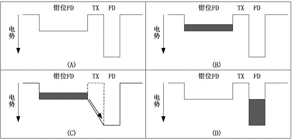
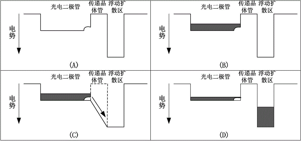
technical field [0001] The invention belongs to the technical field of microelectronics, and in particular relates to a silicon-based CMOS image sensor and a method for suppressing recombination of photogenerated carrier surface traps. Background technique [0002] Image sensors are semiconductor devices that convert optical images into electrical signals, and can generally be divided into CMOS image sensors and CCD image sensors. CMOS image sensor has been the research hotspot of image sensor in the past ten years. Compared with traditional CCD image sensor, CMOS image sensor has the advantages of small size, low power consumption and low cost, and because of its compatibility with CMOS process, CMOS image sensor A powerful system-on-chip can be realized. [0003] A single pixel of a conventional CMOS image sensor such as figure 1 shown. It consists of a photodiode (PPD), a floating diffusion (FD) and a transfer transistor (TX). [0004] Ideally, the working principle o...

Claims


Application Information

Patent Timeline
Patent Type & Authority Applications(China)
IPC IPC(8): H01L27/146
Inventor 蒋玉龙包永霞
Owner FUDAN UNIV
Why Eureka
Try Eureka