CdS organic electroluminescence device
An electroluminescent device and a technology for light-emitting devices, which are applied to the field of light-emitting devices in the field of white light illumination, can solve the problems of decreased device efficiency, low device efficiency, concentration quenching, etc., and achieve the effects of improving brightness and efficiency.
- Summary
- Abstract
- Description
- Claims
- Application Information
AI Technical Summary
Problems solved by technology
Method used
Image
Examples
Embodiment Construction
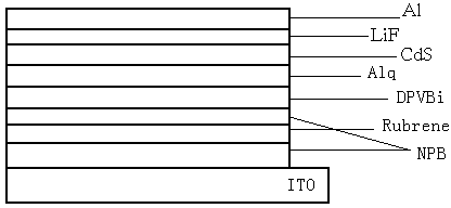
[0025] attached by figure 1 Shown: The light-emitting device includes ITO glass anode substrate (70nm), NPB layer (50nm), Rubrene layer (0.2nm), NPB layer (5nm), DPVBi layer (30nm), Alq3 layer (30nm) from bottom to top , LiF layer (0.5nm) and Al cathode layer (100nm ~ 120nm) layer, characterized in that: it also includes a CdS electron injection layer (0.1nm), the CdS electron injection layer is arranged between the Alq3 layer and the LiF layer between;
[0026] The preparation process is as follows: using ITO glass as the anode substrate, the ITO glass is repeatedly scrubbed with acetone, ethanol, and deionized water, ultrasonically, and finally dried; the device is prepared in a multi-source organic molecule vapor deposition system, and the materials used are respectively Placed in different evaporation sources, the temperature of each evaporation source can be controlled separately, and the evaporation of NPB layer, Rubrene layer, NPB layer, DPVBi layer and Alq3 layer is c...
PUM
 Abstract
Description
Claims
Application Information


